TSMC vs Intel vs Samsung: The Race to 1.4nm Chips
Key Takeaways
- All three foundries started 2nm production between mid-2025 and December 2025
- Intel pursues the most aggressive roadmap with simultaneous GAA transistors and backside power delivery
- Samsung prioritizes yield improvement over breakthrough scaling after SF2 launch
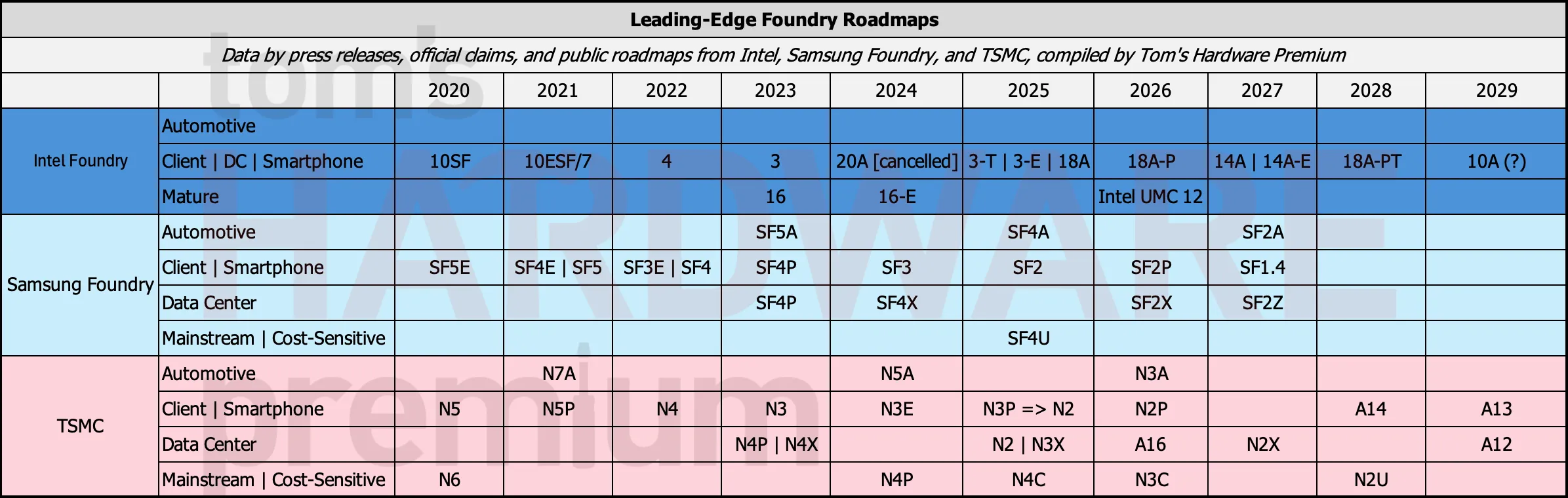
The semiconductor industry just hit a milestone. All three companies capable of manufacturing leading-edge chips have started producing 2nm-class processors within a six-month window.
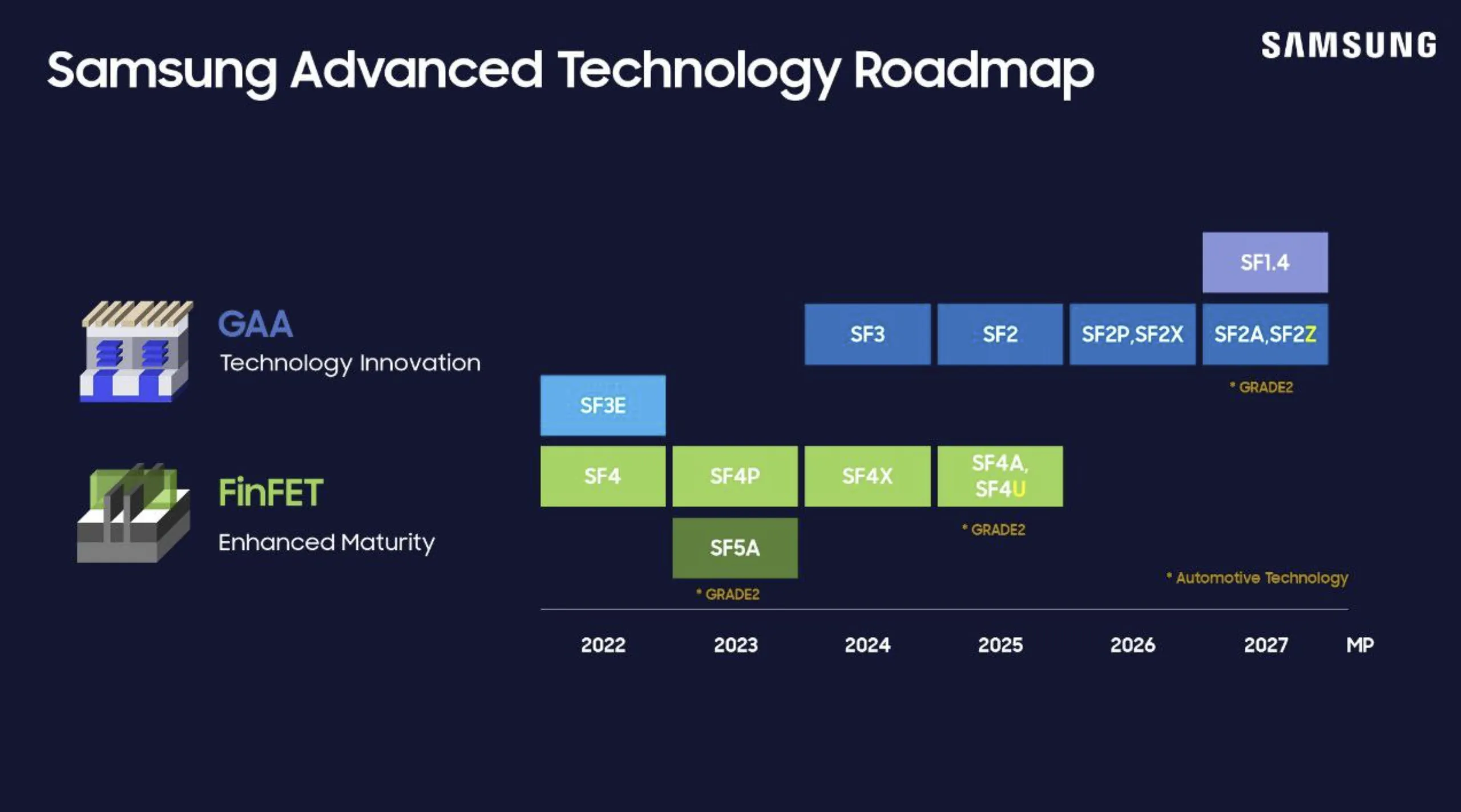
Samsung fired first with its SF2 node around mid-2025. Intel followed in November with 18A production at its Oregon development lines. TSMC completed the trio in December, launching high-volume manufacturing of N2 chips at two Taiwan fabs.
What comes next separates these three companies more than their current nodes. Their roadmaps to 1.4nm and beyond reveal fundamentally different bets on technology, timing, and risk.
Why Only Three Companies Can Build These Chips
The capital, expertise, and experience required to develop leading-edge processes and build supporting fabs has narrowed the field to TSMC, Intel, and Samsung. Companies like Rapidus have yet to prove they can compete at this level.
All three foundries are shifting from traditional node scaling to a segmented, product-driven approach. But their priorities differ sharply.
Intel: Biggest Gamble, Biggest Potential Payoff
Intel's roadmap is the most ambitious and the most volatile. As both a foundry and an integrated design manufacturer, Intel needs cutting-edge fabrication to differentiate its own consumer and data center products.
The company bet on simultaneous implementation of two major technologies: gate-all-around (GAA) RibbonFET transistors and PowerVia backside power delivery network (BSPDN). Most competitors are adopting these technologies sequentially. Intel is doing both at once with 18A.
Intel also plans aggressive pursuit of High-NA EUV lithography in 2027 to 2028. That's years before rivals expect to adopt this next-generation patterning technology.
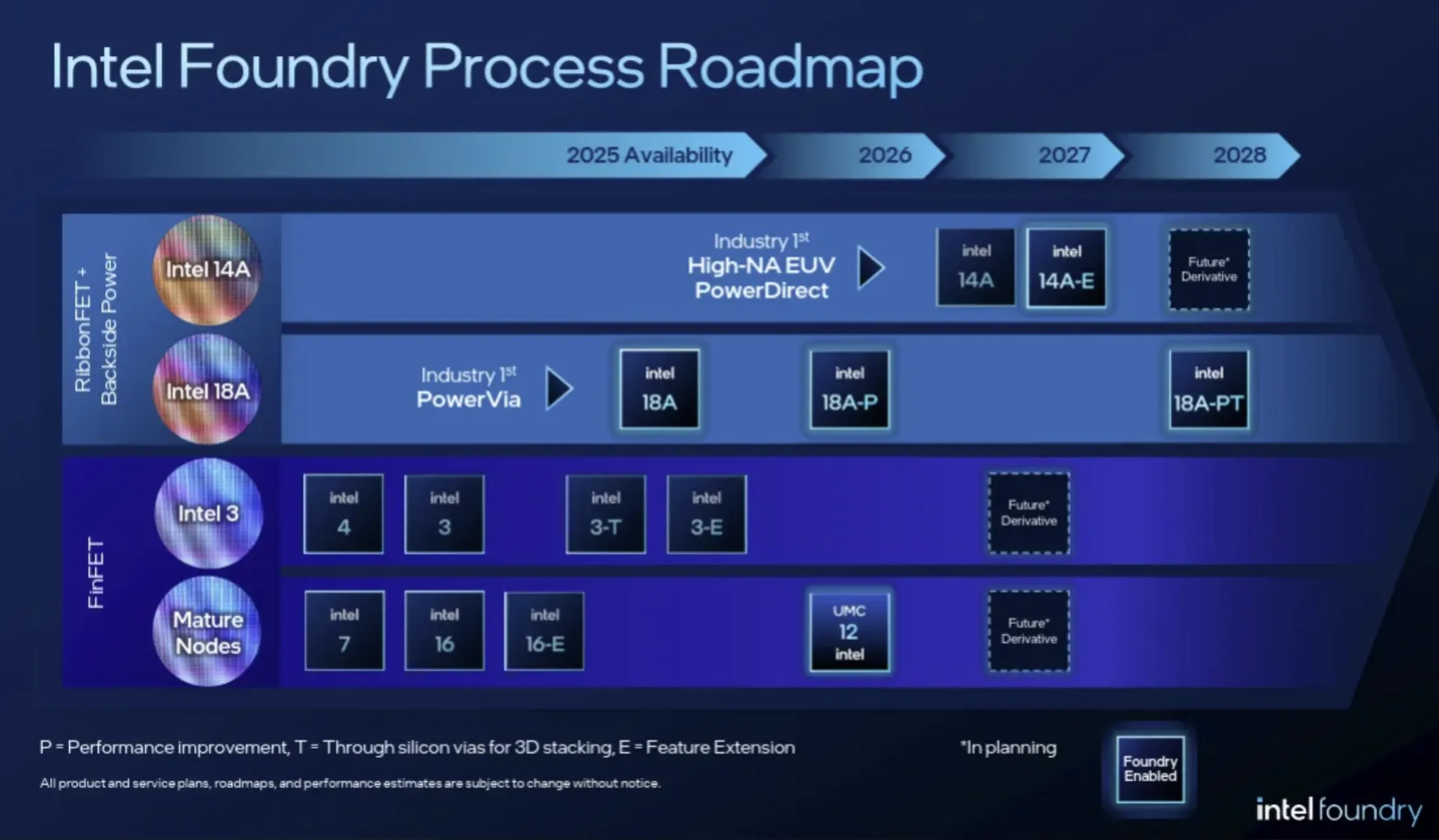
The risk: Intel's 18A production started at development lines in Oregon, not the production lines in Arizona intended for volume manufacturing. Whether the company can translate development success into high-volume yields remains unproven.
TSMC: Predictable Scaling With Strategic Splits
TSMC's approach prioritizes predictability and specialization over technological firsts. The company split its roadmap into two tracks: high-performance computing nodes with backside power delivery, and cost-optimized nodes without it.
This segmentation lets TSMC serve different customer needs. AI accelerator designers who need maximum performance can pay for BSPDN. Mobile chip makers who prioritize cost and density can use simpler processes.
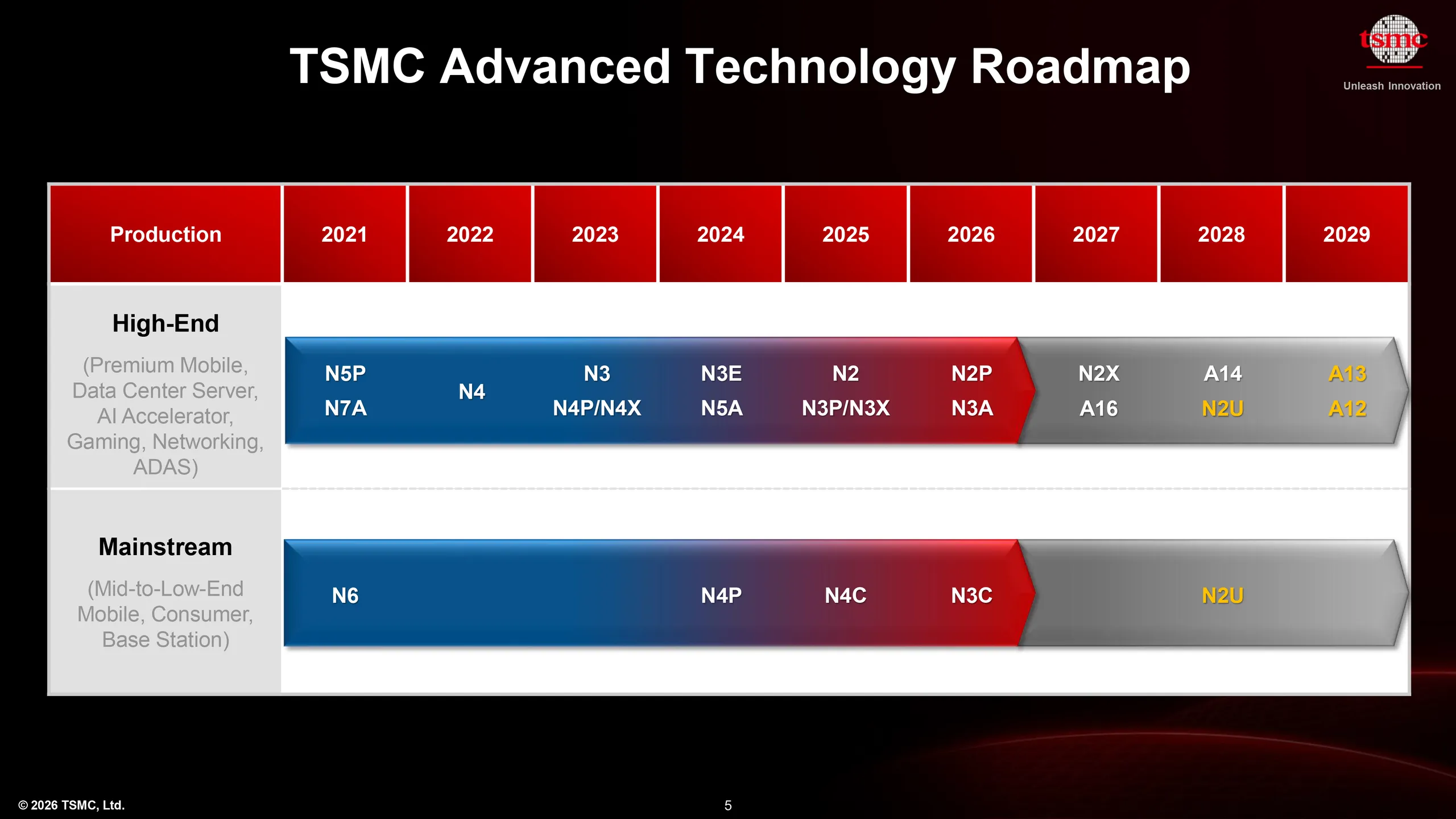
TSMC's December N2 launch at two volume fabs signals confidence in yields. Starting at multiple production facilities rather than a single pilot line suggests the company has already worked through major manufacturing challenges.
Samsung: Fixing Yields Before Chasing Breakthroughs
Samsung launched SF2 first but faces questions about whether it's a genuine new node or a rebadged version of SF3P. The company offers a wide range of node variants, but its current focus is yield improvement rather than scaling.
This pragmatic approach explains why Samsung trails competitors on backside power delivery implementation. The company appears to be prioritizing reliable production of current nodes over racing to adopt new architectures.
Samsung's roadmap looks more iterative than breakthrough-focused. For customers who value predictable delivery over bleeding-edge specs, that may be the right trade-off.
The Technology Bets That Matter
Three technologies will determine who leads at 1.4nm and beyond: gate-all-around transistors, backside power delivery, and High-NA EUV lithography.
- GAA transistors: All three foundries are adopting this architecture, which replaces FinFET designs. Intel calls its version RibbonFET.
- Backside power delivery (BSPDN): Routes power through the back of the chip, freeing up space for signals on the front. Intel leads with PowerVia; TSMC is splitting its roadmap around this feature; Samsung lags.
- High-NA EUV: The next generation of extreme ultraviolet lithography. Intel plans adoption in 2027-2028, well ahead of rivals.
Intel's simultaneous adoption of GAA and BSPDN is the riskiest approach. If it works, Intel could leapfrog competitors. If yields suffer, the company could fall further behind.
| Feature | Intel | TSMC | Samsung |
|---|---|---|---|
| 2nm Production Start | November 2025 (dev lines) | December 2025 (volume) | Mid-2025 |
| GAA Transistors | RibbonFET (18A) | N2 and beyond | SF2 and beyond |
| Backside Power Delivery | PowerVia (18A) | Split roadmap (HPC only) | Behind competitors |
| High-NA EUV Timeline | 2027-2028 | Later than Intel | Later than Intel |
What This Means for Chip Buyers
Companies designing chips face a strategic choice. TSMC offers the safest path with proven yields and flexible node options. Intel offers the most advanced technology for those willing to accept execution risk. Samsung offers competitive pricing and a company focused on production reliability over feature races.
The foundry you choose for a 2026 tapeout will depend on whether you prioritize time-to-market, absolute performance, or cost. No single foundry dominates all three.
Logicity's Take
Frequently Asked Questions
Which foundry started 2nm production first?
Samsung began SF2 production around mid-2025, followed by Intel's 18A in November and TSMC's N2 in December 2025.
What is backside power delivery and why does it matter?
Backside power delivery routes electrical power through the back of a chip instead of the front. This frees up space for signal routing, improving performance and density. Intel leads with its PowerVia implementation.
When will 1.4nm chips be available?
Intel plans High-NA EUV adoption in 2027-2028, which would enable 1.4nm-class production. TSMC and Samsung expect to reach this milestone later.
Why can only three companies make leading-edge chips?
The capital, expertise, and experience required to develop advanced process technologies and build supporting fabs is so high that only TSMC, Intel, and Samsung can currently compete.
Is Samsung's SF2 a real new node?
There's debate about whether SF2 is a genuinely new process or a rebadged version of SF3P. Samsung's current focus appears to be yield improvement rather than breakthrough scaling.
Need Help Implementing This?
Source: Latest from Tom's Hardware
Manaal Khan
Tech & Innovation Writer
Related Articles
Browse all
Alienware AW2726DM Review: The $350 QD-OLED Gaming Monitor That Changes Everything
Dell's Alienware AW2726DM shatters the OLED gaming monitor price barrier at just $350, delivering 27-inch QHD resolution, 240Hz refresh rate, and Quantum Dot color that rivals monitors costing twice as much. This isn't an incremental price drop. It's a complete reset of what budget-conscious gamers can expect.

iPhone Fold Launch 2026: Apple's First Foldable Could Capture 19% Market Share Instantly
Apple's long-awaited foldable iPhone is finally coming, and analysts predict it'll rocket the company to third place in the foldable market behind Samsung and Huawei. The secret weapon? Some seriously clever material science that could solve the crease problem that's plagued every foldable phone so far.

FAA Approves Military Laser Weapons for Drone Defense: What the New Airspace Rules Mean for Border Security
The FAA has given the Pentagon full approval to use high-energy laser systems against drones in US airspace, ending a two-month standoff that started when lasers shot down party balloons mistaken for cartel drones. The decision comes after safety assessments concluded these weapons don't pose increased risk to civilian aircraft.
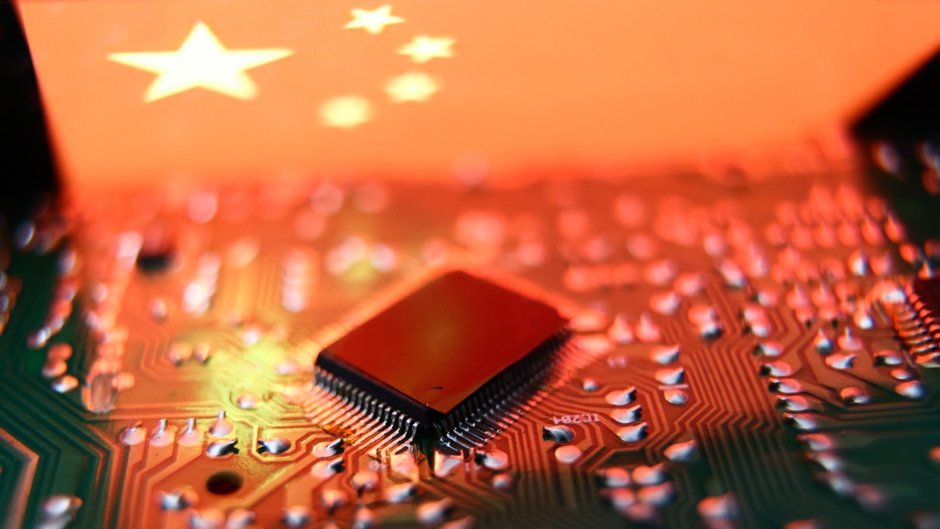
China Chip Subsidies Reach $142 Billion: 3.6x More Than US Spent on Semiconductor Manufacturing
A new CSIS report reveals China has poured $142 billion into semiconductor subsidies over the past decade, dwarfing US spending by a factor of 3.6. But here's the twist: despite this massive investment, Chinese chipmakers still lag years behind TSMC and struggle with abysmal yields at advanced nodes.
Also Read

Turn Obsidian Notes Into Google Slides With Gemini
A workflow combining Obsidian's plain-text notes with Google Gemini can skip the blank-slide problem entirely. Your research notes already have structure. Gemini just converts it into a presentation deck.
Why Windows 11 Registry Tweaks Still Matter After April Update
Microsoft's April 2026 update brought performance fixes and a cleaner Settings app to Windows 11. But power users still reach for the Registry Editor because the update fixed bugs, not the OS's stubborn lack of customization options.

Anthropic Launches Claude for Small Business With 15 Workflows
Anthropic released Claude for Small Business, a new package that connects Claude directly to QuickBooks, PayPal, HubSpot, and other tools small businesses already use. The product includes 15 ready-to-run workflows for payroll planning, month-end close, invoice chasing, and marketing campaigns.