Key Takeaways

- Samsung Foundry now achieves over 80% yield on its 4nm FinFET process
- The 4nm process serves as the base die for sixth-generation HBM4 memory chips
- Samsung expects improved profitability in the second half of 2025
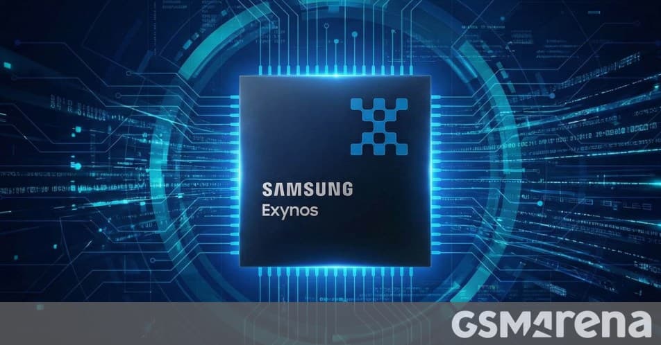
Samsung Foundry has crossed a critical manufacturing threshold. According to a report from South Korean publication SEDaily, the company's 4nm FinFET process now exceeds 80% yield. In semiconductor manufacturing, that number marks the difference between a process that's still being refined and one ready for high-volume production.
The milestone comes six years after Samsung began mass production on the 4nm node. That timeline has drawn criticism from industry observers. TSMC, Samsung's primary competitor in advanced chip manufacturing, typically achieves similar yield rates faster. But reaching 80% now puts Samsung in position to compete for the current wave of AI chip demand.
What This Means for Samsung's Chip Business
Samsung's Pyeongtaek Campus in South Korea produces chips on 5nm, 7nm, and now mature 4nm processes. The company says it's ready to supply 4nm chips to three main markets: AI accelerators, automotive electronics, and mobile devices.
The AI accelerator market matters most right now. Every major tech company is racing to build or buy custom silicon for machine learning workloads. Nvidia, AMD, and a growing list of hyperscalers need foundry capacity. Samsung's improved yields make it a more credible option for these contracts.
There's another angle here. Samsung uses its 4nm process as the base die for sixth-generation HBM4 memory chips. HBM (High Bandwidth Memory) stacks memory vertically and connects it directly to processors. It's essential for AI training hardware. By improving 4nm yields, Samsung strengthens both its foundry and memory businesses.
The TSMC Competition
TSMC dominates advanced chip manufacturing. Apple, Nvidia, AMD, and Qualcomm all rely on TSMC for their most advanced processors. Samsung has struggled to win similar customers for its cutting-edge nodes.
The yield gap has been a major reason. When fewer chips pass quality testing, each working chip costs more to produce. Customers pay for that inefficiency, either through higher prices or longer wait times. An 80% yield rate puts Samsung closer to TSMC's typical performance on mature nodes.
Samsung expects this improvement to help the company return to profitability in the second half of 2025. Higher yields mean lower per-chip costs. Combined with rising memory prices, the company sees a path back to growth.
Six Years to Maturity
The timeline deserves scrutiny. Six years of mass production before reaching 80% yield is slow by industry standards. Samsung's 4nm process has been available since 2022 for some customers, but the company has been refining the technology since earlier development phases.
Part of the challenge stems from Samsung's decision to pursue a different technical approach than TSMC. Both companies use FinFET transistor architecture at 4nm, but their implementations differ. Samsung's bet hasn't paid off as quickly as hoped.
Still, reaching maturity now positions Samsung for the next several years of production. Many chips don't need the absolute latest manufacturing node. A reliable, cost-effective 4nm process can serve automotive, industrial, and mid-range mobile customers well.
Logicity's Take
What Comes Next
Samsung is already working on 3nm and 2nm processes using Gate-All-Around (GAA) transistor architecture. These nodes promise better power efficiency and performance than FinFET designs. Samsung beat TSMC to market with GAA at 3nm, though yield and performance questions remain.
The 4nm milestone suggests Samsung's manufacturing teams are improving their execution. Whether those gains translate to faster ramps on newer nodes will determine the company's foundry future.
Another major hardware manufacturing shift from a tech giant
Frequently Asked Questions
What does chip yield rate mean?
Yield rate measures the percentage of chips that pass quality testing after manufacturing. Higher yields mean lower costs per working chip and more efficient production.
How does Samsung's 4nm process compare to TSMC's?
Both use FinFET transistor architecture, but TSMC generally achieves higher yields faster. Samsung's 80% yield puts it closer to competitive parity on this node.
What is HBM4 memory?
HBM4 is the sixth generation of High Bandwidth Memory, which stacks memory chips vertically for faster data transfer. It's critical for AI training hardware. Samsung uses its 4nm process for HBM4's base die.
Why did Samsung's 4nm process take six years to mature?
Samsung pursued a different technical implementation than TSMC. The approach proved more difficult to optimize, resulting in lower initial yields and a longer path to process maturity.
Which companies use Samsung's 4nm foundry services?
Samsung manufactures chips for various mobile, automotive, and AI accelerator clients. Specific customers aren't always disclosed, but Samsung competes with TSMC for major semiconductor design companies.
Need Help Implementing This?
Source: GSMArena.com / Michail
Manaal Khan
Tech & Innovation Writer
Produced with AI assistance and reviewed by the Logicity editorial team. Learn more in our Editorial Policy.