Key Takeaways
- Anderon will be the world's first pure-play quantum chip foundry, operating a 300mm wafer fab in Albany, New York
- The $2 billion investment splits evenly between CHIPS Act federal funding and IBM cash
- Eight other quantum companies received CHIPS Act awards totaling $1 billion, including GlobalFoundries, D-Wave, and Rigetti
A TSMC for Quantum Computing
IBM announced it will spin off Anderon, a standalone company that will become America's first pure-play quantum chip foundry. The facility, headquartered in Albany, New York, will operate a 300mm quantum wafer fab and offer manufacturing services to competing quantum hardware vendors.
The deal combines a proposed $1 billion CHIPS Act R&D award from the U.S. Department of Commerce with a matching $1 billion cash investment from IBM. This makes Anderon the centerpiece of a broader $2.013 billion federal quantum portfolio split across nine companies, the largest single quantum R&D commitment in U.S. history.
“By establishing Anderon as a standalone foundry, we are not just scaling IBM's own quantum roadmap; we are creating the essential infrastructure for the entire U.S. quantum ecosystem to move from experimental prototypes to real-world, commercial-scale production.”
— Arvind Krishna, Chairman and CEO of IBM
The model IBM is pursuing mirrors TSMC's role in traditional semiconductors: a neutral third-party manufacturer that fabricates chips for multiple customers, including competitors. No such foundry exists anywhere in the quantum computing world today. Every operational quantum computer has been built by a vertically integrated company that designs, fabricates, and operates its own hardware.
The Nine-Company Federal Package
IBM's $1 billion award accounts for roughly half of the entire Department of Commerce quantum package. GlobalFoundries received a separate $375 million allocation to launch a "Quantum Technology Solutions" foundry covering multiple qubit architectures, including superconducting, trapped-ion, photonic, and silicon-spin designs.
The remaining seven recipients each received smaller awards:
- D-Wave: $100 million
- Rigetti: $100 million
- Atom Computing: $100 million
- Infleqtion: $100 million
- PsiQuantum: $100 million
- Quantinuum: $100 million
- Diraq (Australian silicon-spin startup): up to $38 million
Those seven non-foundry companies are required to give the federal government a minority, non-controlling equity stake in exchange for funding. Rigetti disclosed in a memorandum of understanding that the government will receive common stock at a 15% discount. GlobalFoundries separately disclosed a 1% federal equity stake.
IBM's announcement contains no equivalent equity-stake disclosure for Anderon. This is a notable omission given that the Trump administration converted part of Intel's CHIPS Act manufacturing award into a roughly 10% government equity stake last year.
Why 300mm Wafers Matter
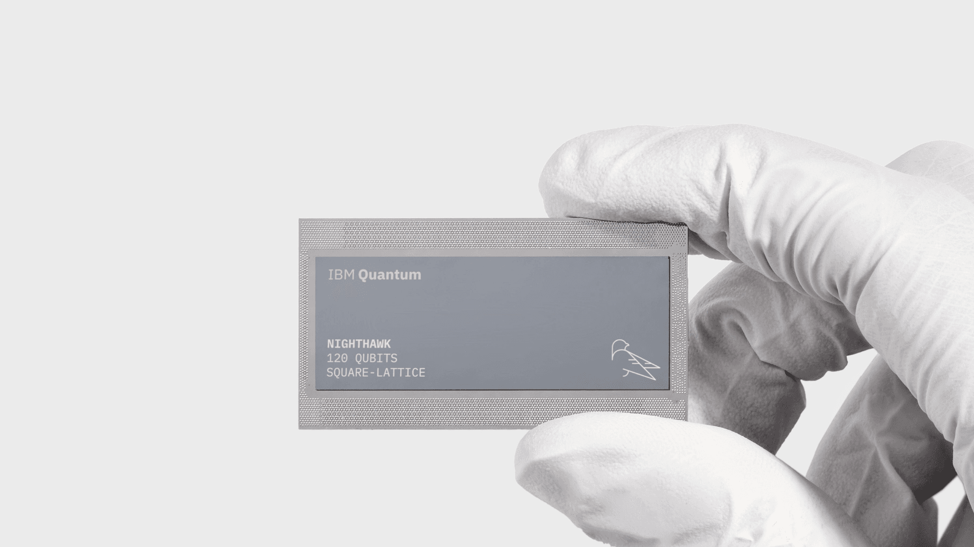
IBM said back in November that all of its current and upcoming quantum processors are built on 300mm silicon wafers at the Albany NanoTech Complex, the largest public-private semiconductor R&D facility operated by the nonprofit NY CREATES.
Jay Gambetta, IBM's Director of Research, wrote that the shift from 200mm to 300mm produces device output roughly 30 times faster by multiplying device complexity tenfold and tripling devices per line. IBM's current production processor, Heron r2, holds 156 fixed-frequency qubits.
Bridging the 'Valley of Death'
The foundry model aims to solve a fundamental problem in quantum computing: the gap between laboratory-scale fabrication and mass production. By leveraging existing semiconductor infrastructure in Albany and federal funding, Anderon will provide standardized manufacturing services to hardware vendors who currently have no external fab option.
Discussion on r/quantumcomputing and Hacker News has focused on whether a foundry model can handle the unique integration challenges of superconducting qubits compared to CMOS processes. Many engineers expressed optimism about the CHIPS Act finally supporting quantum infrastructure beyond just R&D grants.
Logicity's Take
Frequently Asked Questions
What is Anderon?
Anderon is a standalone quantum chip foundry being spun off from IBM, headquartered in Albany, New York. It will operate a 300mm quantum wafer fab and offer manufacturing services to competing quantum hardware vendors.
How much funding does Anderon have?
Anderon is backed by $2 billion in combined funding: a proposed $1 billion CHIPS Act R&D award from the U.S. Department of Commerce and a matching $1 billion cash investment from IBM.
Why is a quantum foundry significant?
No pure-play quantum foundry exists anywhere in the world today. Every operational quantum computer has been built by vertically integrated companies. Anderon would allow hardware vendors to outsource fabrication, similar to how TSMC serves the broader semiconductor industry.
What other companies received CHIPS Act quantum funding?
GlobalFoundries received $375 million. D-Wave, Rigetti, Atom Computing, Infleqtion, PsiQuantum, and Quantinuum each received $100 million. Australian startup Diraq will receive up to $38 million.
Another breakthrough in advanced computing capabilities
Need Help Implementing This?
Source: Latest from Tom's Hardware
Manaal Khan
Tech & Innovation Writer
Produced with AI assistance and reviewed by the Logicity editorial team. Learn more in our Editorial Policy.