TSMC: CoWoS can pack 58 dies before panels take over
Key Takeaways
- TSMC can scale CoWoS to integrate 58 large dies in a single package using existing wafer-level processes
- Panel-based CoPoS won't reach high-volume manufacturing until 2028-2029 at earliest
- Wafer-level tools remain far more advanced than panel-level alternatives across the industry
TSMC's wafer-level packaging technology, CoWoS, can scale to integrate 58 massive dies in a single package. The company isn't ready to hand the future of AI chip packaging to panel-based alternatives anytime soon. Kevin Zhang, TSMC's senior vice president of business development, made this clear at the company's European Technology Symposium.
The semiconductor industry has been buzzing about panel-level packaging as the next frontier. Panels offer dramatically larger surface area, up to 750mm×620mm compared to the 300mm circular wafers used today. Bigger panels should mean bigger chips, which should mean more powerful AI processors. The logic seems straightforward.
TSMC disagrees with the urgency.
Why TSMC says wafer-level packaging still has runway
Zhang's position is blunt: wafer-level processes are simply more advanced than anything panel-based manufacturing can offer today. "The geometry complexity panel-based process has to deal with is nowhere near the wafer level technology capability," he said. This isn't a TSMC-specific advantage. It's an industry-wide reality.
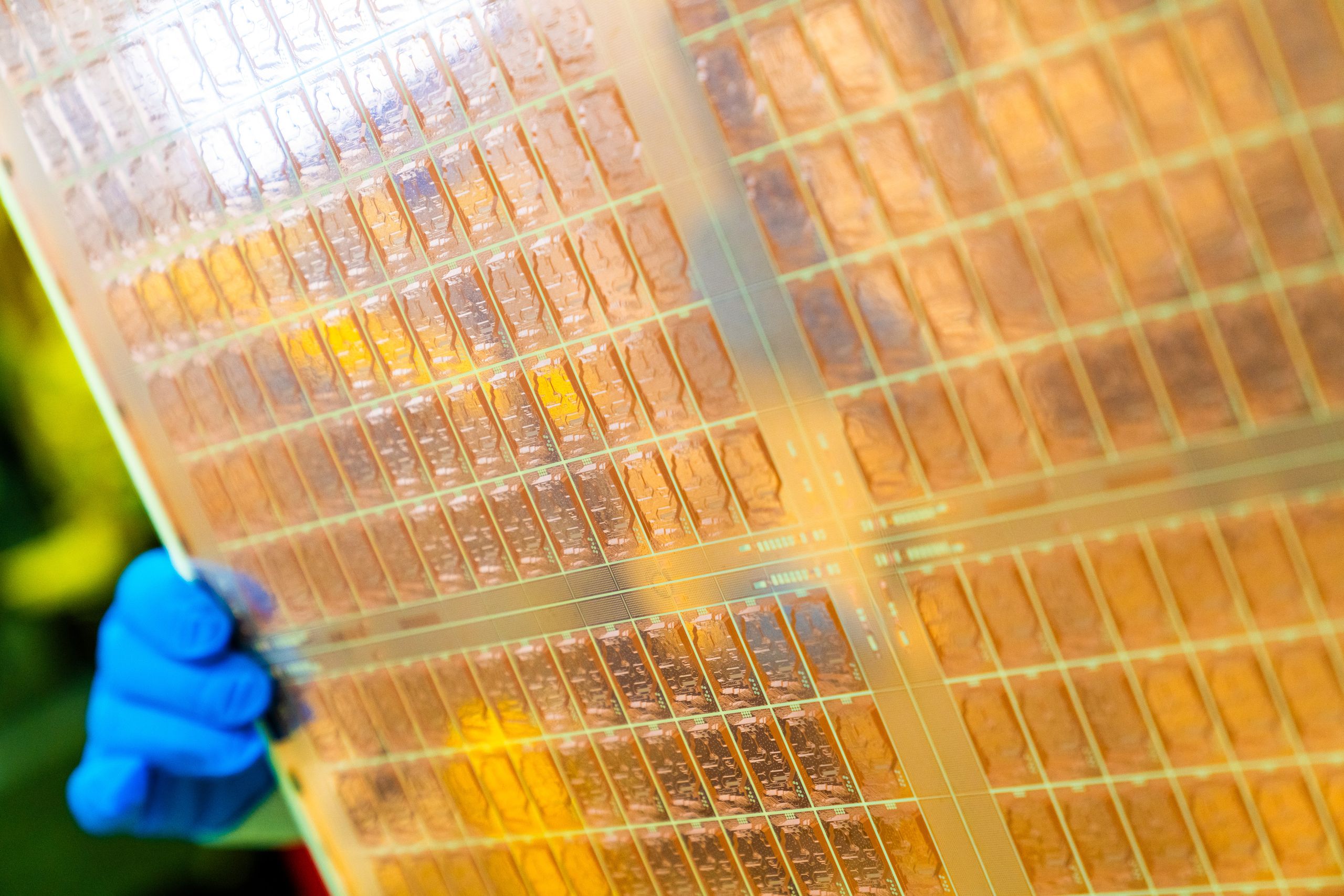
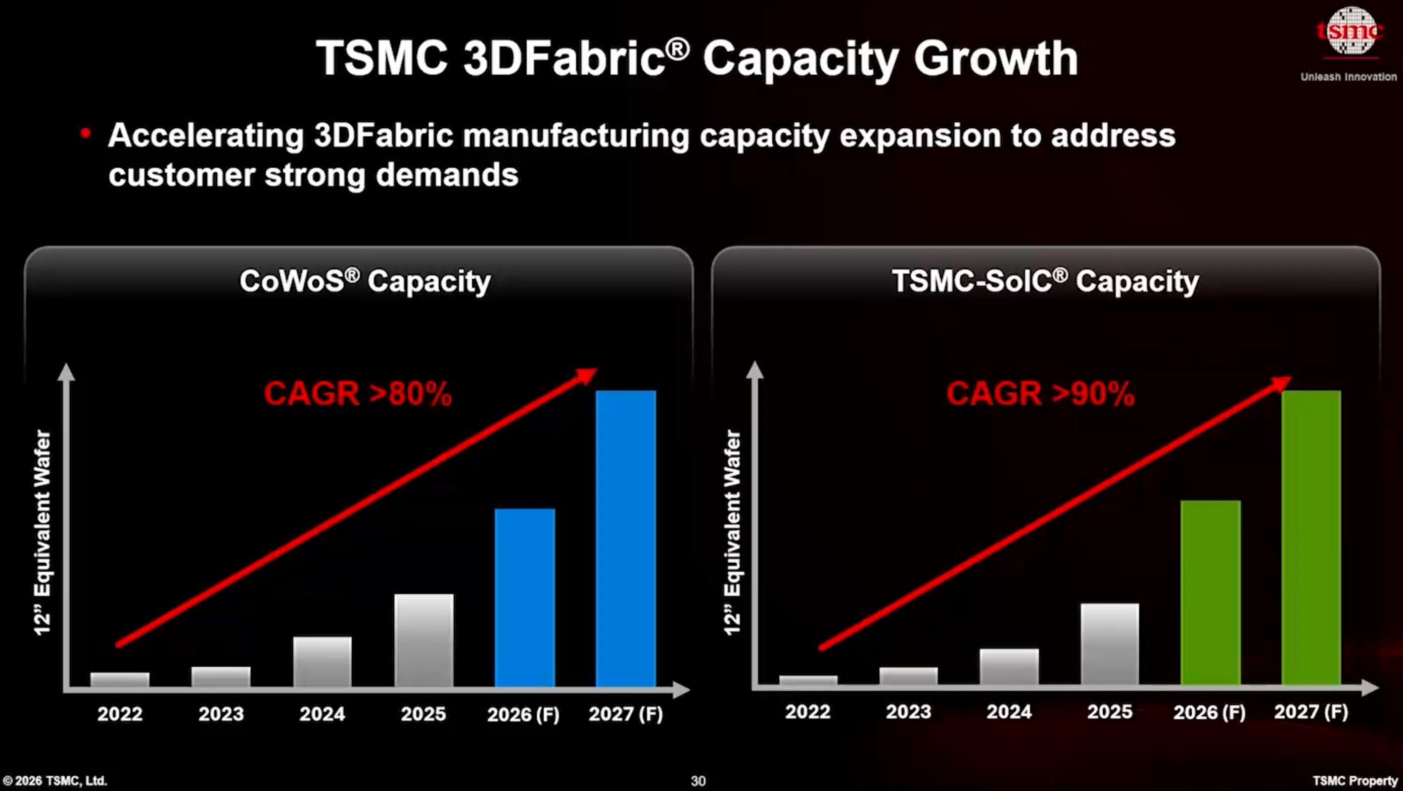
CoWoS, which stands for Chip-on-Wafer-on-Substrate, uses the same lithography, etching, and deposition tools that make leading-edge logic chips. These tools have been refined over decades. Panel-level tools, by comparison, are starting from a much earlier point on the maturity curve.
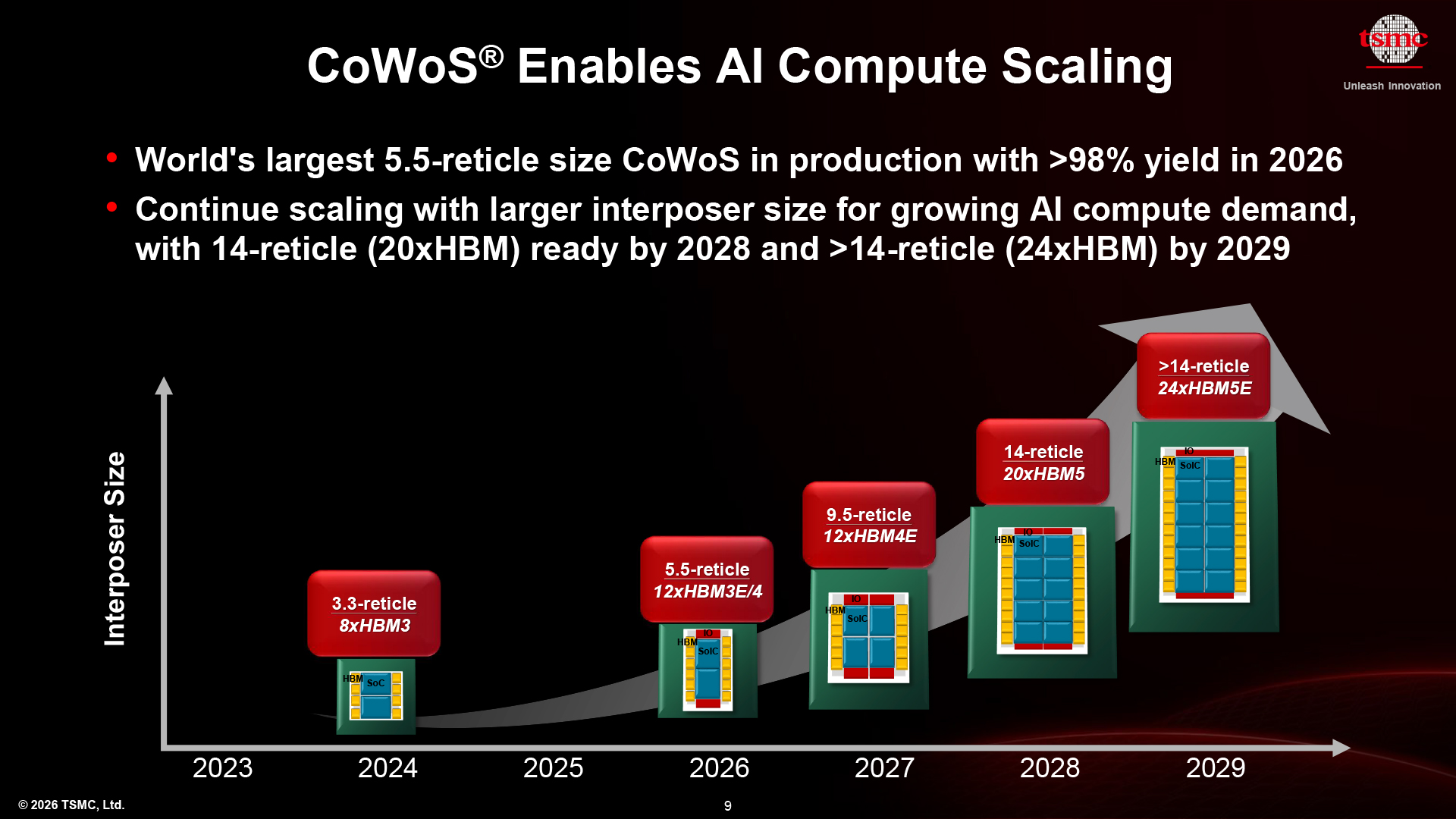
TSMC's current CoWoS roadmap extends to what the company calls "14X" using wafer-level processes. That means integrating up to 58 large reticle-sized dies, the maximum size that can be printed in a single lithography exposure, into one package. For context, Nvidia's current flagship AI chips use CoWoS to connect multiple dies. TSMC is saying they can scale this approach roughly tenfold before hitting fundamental limits.
What panels actually offer
Panel-level packaging does have one clear advantage: size. TSMC's current CoWoS substrates measure 120mm×150mm. Next-generation versions will expand to 150mm×250mm. But even that looks modest next to panel dimensions. Initial panels start at 310mm×310mm, with future generations reaching 515mm×510mm or 750mm×620mm.
That's roughly 300% more usable area compared to circular 300mm wafers. More area means more dies, more memory, and more interconnects in a single package. For AI systems that need to shuttle enormous amounts of data between processing units and memory, bigger packages could translate directly to better performance.
But size isn't everything. Interconnection density, the number of signal paths per unit area, matters just as much. Zhang's point is that panel-based processes can't yet match the interconnect density of wafer-level packaging. Until they can, panels will complement CoWoS rather than replace it.
When will CoPoS actually ship?
TSMC expects to complete its first CoPoS (Chip-on-Panel-on-Substrate) pilot line this June. But a pilot line is a long way from products on shelves. The typical gap between pilot and high-volume manufacturing runs two to three years. That puts realistic CoPoS HVM at 2028 or 2029.
Even that timeline may be optimistic. CoPoS requires new tools, and the industry doesn't yet know all the quirks of scaling panel-based processes. A more conservative estimate puts the first CoPoS-based products in 2029 or 2030, with meaningful volumes arriving in the first half of the next decade.
There's a precedent for this slow adoption curve. CoWoS itself existed for years before demand exploded with the AI boom. CoPoS will likely follow the same pattern: available in limited quantities for niche applications before mainstream adoption catches up.
What this means for AI chip buyers
For companies building or buying AI infrastructure in the next three to four years, the message is clear: plan around CoWoS. The technology has proven manufacturing scale, and TSMC is committed to pushing it further. Panel-based packaging will eventually arrive, but it won't be the primary option for flagship AI processors until the late 2020s at earliest.
This also suggests Nvidia, AMD, and other TSMC customers designing chips for 2026-2028 launches are likely targeting CoWoS variants rather than waiting for CoPoS. The performance and density advantages of wafer-level packaging outweigh the size benefits of panels, at least for now.
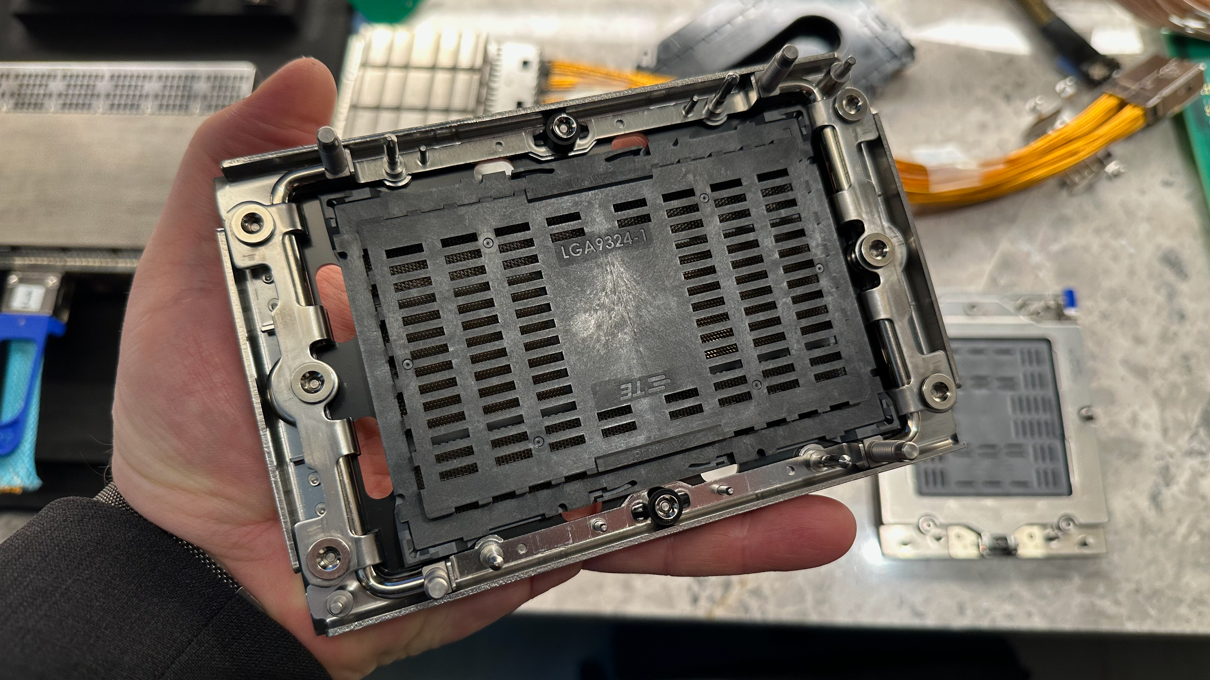
The power demands of next-gen AI processors require new socket designs to match advanced packaging
Logicity's Take
TSMC's 58-die claim is as much a negotiating position as a technical statement. By signaling years of CoWoS headroom, TSMC is telling customers not to bet on panel packaging from competitors like Intel or Samsung. The subtext: stick with us, we have the roadmap. Whether panel processes from rivals can leapfrog TSMC's wafer-level lead will determine if this confidence holds.
Frequently Asked Questions
What is CoWoS packaging?
CoWoS (Chip-on-Wafer-on-Substrate) is TSMC's advanced packaging technology that connects multiple chiplets on a silicon interposer, enabling high-bandwidth communication between dies. It's used in Nvidia's flagship AI GPUs and other high-performance processors.
How is CoPoS different from CoWoS?
CoPoS (Chip-on-Panel-on-Substrate) uses rectangular panels instead of circular wafers as the base substrate. Panels offer more surface area but currently lack the interconnection density of wafer-level processes.
When will panel-based AI chips be available?
TSMC expects high-volume manufacturing of CoPoS-based products between 2028-2030, with meaningful adoption likely in the first half of the 2030s.
Why can panels be larger than wafers?
Wafers are circular and limited to about 300mm diameter by manufacturing constraints. Panels are rectangular substrates that can scale to 750mm×620mm, offering roughly 300% more usable area.
Will CoPoS replace CoWoS entirely?
No. TSMC indicates CoPoS will complement CoWoS rather than replace it. Different products will benefit from different packaging approaches depending on their density and size requirements.
Need Help Implementing This?
If you're planning AI infrastructure and need to understand how chip packaging decisions affect your deployment timeline or vendor choices, reach out to Logicity's editorial team. We connect readers with analysts who track semiconductor supply chains and can provide tailored guidance.
Source: Latest from Tom's Hardware
Huma Shazia
Senior AI & Tech Writer
Related Articles
Browse all
Alienware AW2726DM Review: The $350 QD-OLED Gaming Monitor That Changes Everything
Dell's Alienware AW2726DM shatters the OLED gaming monitor price barrier at just $350, delivering 27-inch QHD resolution, 240Hz refresh rate, and Quantum Dot color that rivals monitors costing twice as much. This isn't an incremental price drop. It's a complete reset of what budget-conscious gamers can expect.
iPhone Fold Launch 2026: Apple's First Foldable Could Capture 19% Market Share Instantly
Apple's long-awaited foldable iPhone is finally coming, and analysts predict it'll rocket the company to third place in the foldable market behind Samsung and Huawei. The secret weapon? Some seriously clever material science that could solve the crease problem that's plagued every foldable phone so far.
FAA Approves Military Laser Weapons for Drone Defense: What the New Airspace Rules Mean for Border Security
The FAA has given the Pentagon full approval to use high-energy laser systems against drones in US airspace, ending a two-month standoff that started when lasers shot down party balloons mistaken for cartel drones. The decision comes after safety assessments concluded these weapons don't pose increased risk to civilian aircraft.
China Chip Subsidies Reach $142 Billion: 3.6x More Than US Spent on Semiconductor Manufacturing
A new CSIS report reveals China has poured $142 billion into semiconductor subsidies over the past decade, dwarfing US spending by a factor of 3.6. But here's the twist: despite this massive investment, Chinese chipmakers still lag years behind TSMC and struggle with abysmal yields at advanced nodes.