Key Takeaways
- 3D X-DRAM achieved sub-10 nanosecond read/write latency in proof-of-concept testing
- The technology uses existing 3D NAND manufacturing equipment, potentially reducing fabrication costs
- Acer founder Stan Shih led a new strategic investment round in NEO Semiconductor
NEO Semiconductor announced on April 23 that its 3D X-DRAM technology passed proof-of-concept validation. The company claims the technology represents a new class of high-density DRAM that can be manufactured using existing 3D NAND infrastructure. If the approach scales, it could offer an alternative to HBM for AI processor memory.
The announcement came alongside news of a strategic investment led by Stan Shih, the founder and former Chairman and CEO of Acer. Shih also served as a board director at TSMC for over two decades.
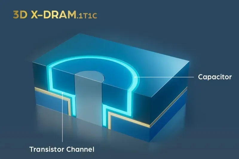
What Is 3D X-DRAM?
3D X-DRAM uses a vertically stacked architecture designed to break past conventional memory scaling limits. NEO claims the design offers higher density, lower power consumption, and better suitability for AI workloads compared to traditional DRAM.
The key differentiator is the manufacturing approach. NEO's architecture draws heavily on 3D NAND techniques. The company says its POC chips were produced using mature 3D NAND processes, including existing equipment and materials. This matters because advanced memory development often hits walls not in design innovation, but in fabrication cost and process compatibility.

Proof-of-Concept Results
The POC chips were fabricated and tested at Taiwan's National Institutes of Applied Research, Taiwan Semiconductor Research Institute (NIAR-TSRI), in collaboration with National Yang Ming Chiao Tung University. Here's what NEO reported:
- Read/write latency: under 10 nanoseconds
- Data retention: over 1 second at 85°C (NEO claims 15x improvement over JEDEC standard)
- Bit-line disturbance: over 1 second at 85°C
- Word-line disturbance: over 1 second at 85°C
- Endurance: greater than 10¹⁴ cycles
“These results validate a new scaling path for DRAM. We believe this technology can enable significantly higher density, lower cost, and improved energy efficiency for the AI era. By leveraging established 3D NAND manufacturing processes and ecosystem, we aim to bring 3D DRAM to reality sooner.”
— Andy Hsu, Founder & CEO of NEO Semiconductor
The Business Model: Licensing and Partnerships
NEO isn't positioning itself as a memory manufacturer. Hsu said the company is "actively engaging with leading global memory and semiconductor companies on potential co-development opportunities." The plan is a licensing and partnership model rather than direct production.
This approach makes sense given the capital intensity of memory fabrication. If NEO's technology works as claimed, established memory makers like Samsung, SK Hynix, or Micron could license it and integrate the manufacturing approach into their existing 3D NAND fabs.
Why This Matters for AI Hardware
Memory bandwidth is a bottleneck for AI accelerators. HBM (High Bandwidth Memory) currently dominates this space, but it's expensive and supply-constrained. SK Hynix and Samsung can't build HBM fast enough to meet demand from Nvidia and other chip designers.
If 3D X-DRAM can deliver competitive performance using existing 3D NAND production lines, it could ease supply constraints and potentially lower costs. That's a big "if." Proof-of-concept is a long way from volume production.
More on how AI hardware decisions shape tech leadership priorities
What's Next
NEO has validated that the concept works in a lab setting. The company now needs to demonstrate that the technology can scale to production volumes while maintaining performance and yields. That process typically takes years and significant capital.
The Stan Shih investment provides credibility and presumably some of that capital. Shih's track record at Acer and his TSMC board experience suggest he sees genuine potential in the technology. But investors have backed promising memory technologies before that never reached commercial viability.
Logicity's Take
Frequently Asked Questions
What is 3D X-DRAM?
3D X-DRAM is a vertically stacked DRAM architecture developed by NEO Semiconductor. It uses manufacturing techniques borrowed from 3D NAND flash production, potentially allowing high-density memory to be built on existing fab equipment.
How does 3D X-DRAM compare to HBM?
NEO positions 3D X-DRAM as an HBM alternative for AI workloads. The key advantage is manufacturing compatibility with existing 3D NAND processes, which could lower costs and ease supply constraints. Direct performance comparisons aren't available yet.
When will 3D X-DRAM be available?
NEO has only completed proof-of-concept validation. Commercial availability will depend on successful scaling, licensing deals with memory manufacturers, and production ramp-up. No timeline has been announced.
Who invested in NEO Semiconductor?
The strategic investment round was led by Stan Shih, founder and former CEO of Acer, who also served as a TSMC board director for over 20 years.
Need Help Implementing This?
Source: Latest from Tom's Hardware
Huma Shazia
Senior AI & Tech Writer
Produced with AI assistance and reviewed by the Logicity editorial team. Learn more in our Editorial Policy.