Key Takeaways
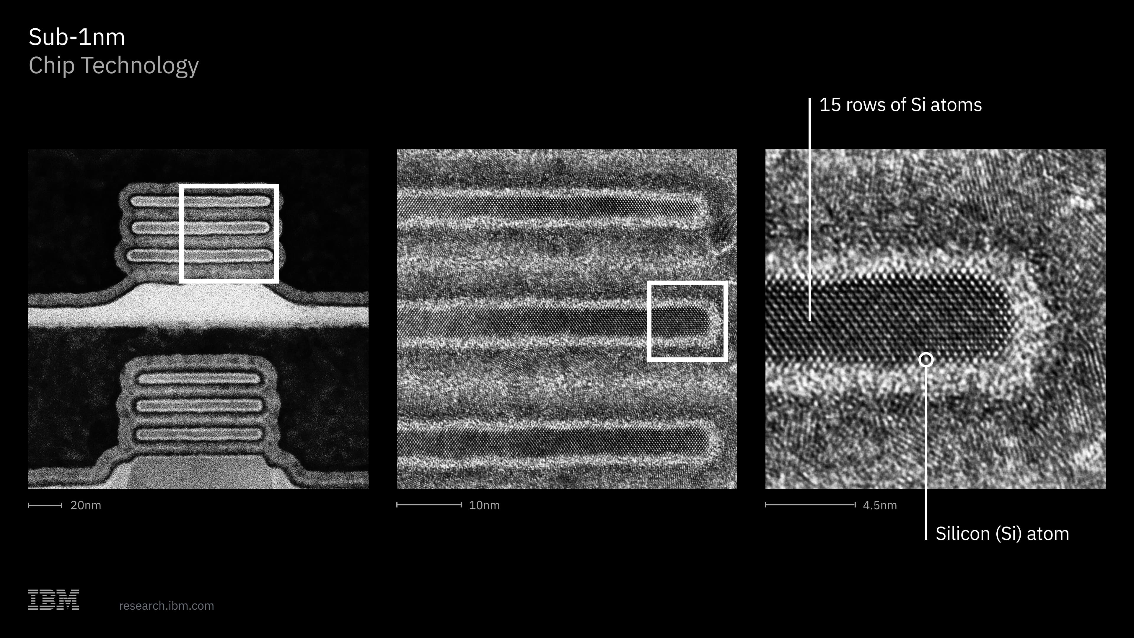
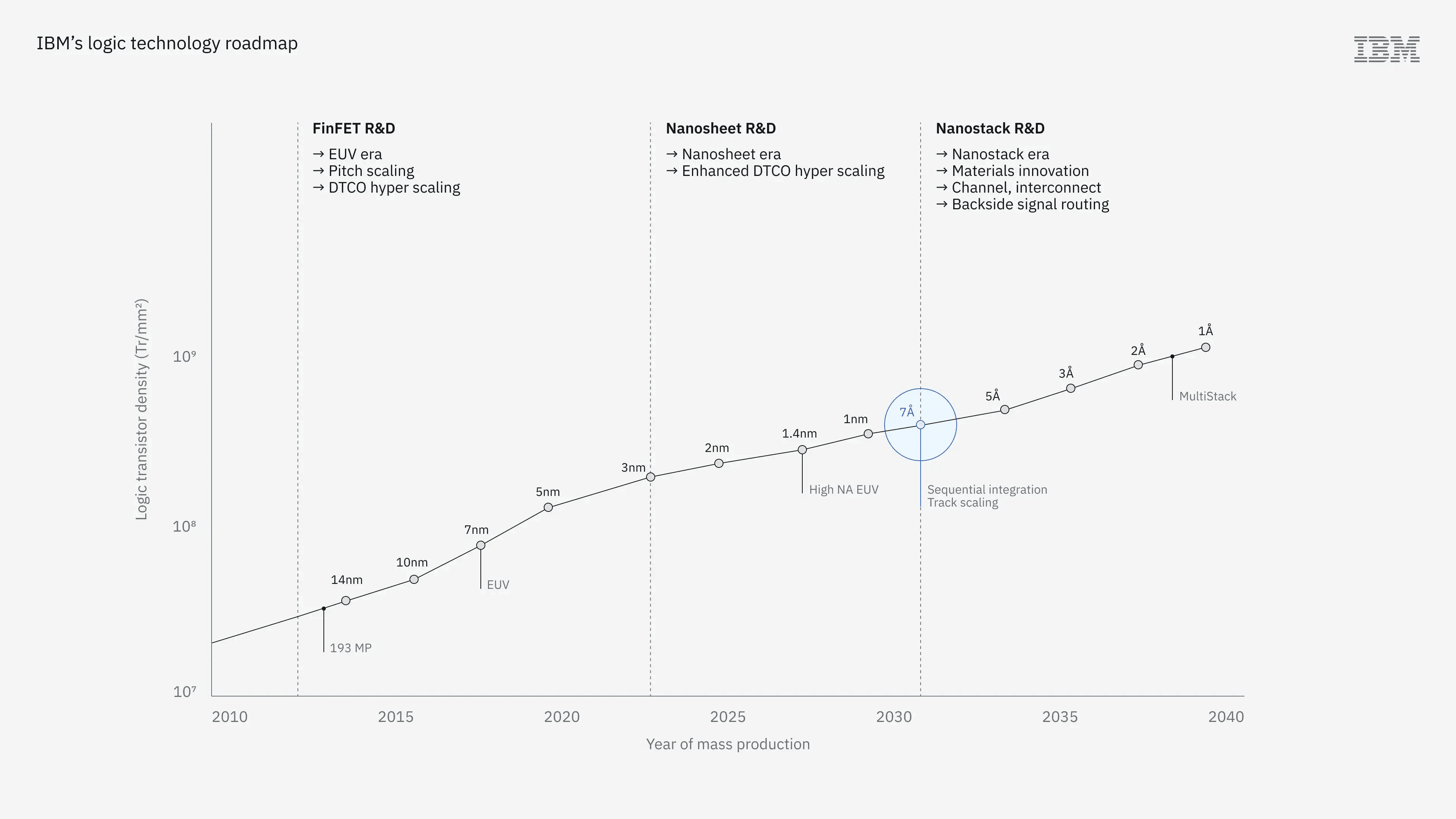
- IBM produced the first test chip using 0.7nm-class (7 angstroms) fabrication, the industry's first sub-1nm process
- The nanostack architecture bonds two wafers together, stacking n-type and p-type transistors vertically instead of side by side
- IBM claims 50% higher performance, 70% better energy efficiency, and 40% higher SRAM density versus its 2nm node
IBM has produced the first test chip using a 0.7nm-class fabrication process, breaking the 1nm barrier with an architecture that stacks transistors vertically across two bonded wafers. The company claims the technology delivers 50% higher performance and 70% better energy efficiency compared to its 2nm-class node from 2021.
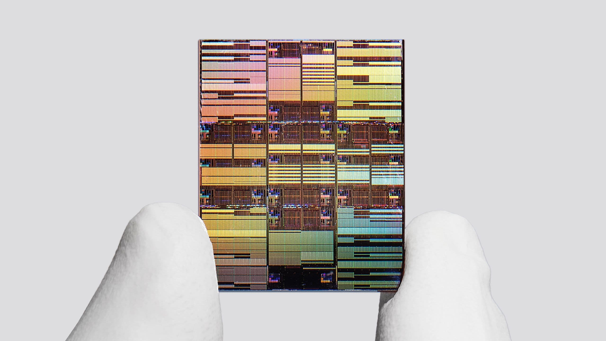
The test chip is about the size of a fingernail. IBM says nothing about manufacturing costs or commercial viability. But the underlying architecture, called nanostack, represents a genuine departure from how transistors have been built for decades.
How does IBM's nanostack architecture work?
Every modern processor uses CMOS logic, which pairs two types of transistors: n-type (NFETs) and p-type (PFETs). Traditionally, these sit side by side on a single wafer, sharing the same layer. As chipmakers shrink transistors generation after generation, this lateral arrangement gets harder to compress.
IBM's nanostack flips the geometry. Instead of placing NFETs and PFETs next to each other horizontally, it stacks them vertically. The company manufactures n-type transistors on one wafer and p-type transistors on another, then bonds the wafers together using an ultra-thin dielectric layer.
This vertical stacking turns a 2D footprint into a 3D structure. IBM claims it roughly doubles transistor density compared to its 2nm research node without the usual planar shrinking that's become increasingly difficult.

Why use two wafers instead of one?
The two-wafer approach solves a longstanding problem: optimizing n-type and p-type transistors requires different conditions. On a single wafer, both transistor types share the same materials and process steps, limiting how much engineers can tune each one independently.
By building them on separate wafers, IBM can use different channel materials, different strain engineering, and different process conditions for each type. Each tier gets optimized on its own terms before the two are bonded together.
The architecture resembles complementary FETs (CFETs), a concept other chipmakers have proposed. But IBM's method differs from monolithic CFETs because it builds the transistor tiers separately rather than growing them sequentially on one wafer.
What are the claimed performance gains?
IBM lists several improvements over its 2nm-class node, which itself used gate-all-around nanosheet transistors and was demonstrated in 2021:
- Up to 50% higher performance
- Up to 70% better energy efficiency
- 40% higher SRAM density
- Even higher density improvements for logic transistors
The SRAM density gain matters. SRAM is notoriously hard to shrink because its six-transistor cell must maintain stability while getting smaller. A 40% improvement suggests the vertical stacking helps with memory cells, not just logic.
What are the manufacturing challenges?
The nanostack approach introduces problems that don't exist with single-wafer processes.
Alignment is critical. Two advanced logic wafers must line up with extreme precision. At this scale, even nanometer-level misalignment between the bonded layers could cause failures. Any defect at the bond interface can kill the entire stack.
Routing and power delivery get more complex when you have two active device tiers. Engineers must figure out how to connect transistors across layers and deliver power to both tiers efficiently.
Cooling is another concern. One active tier now sits farther from the heat sink than it would in a traditional chip. Heat dissipation gets harder when you're stacking more transistors into less space.
Then there's cost. IBM has to pay for two advanced front-end-of-line wafers instead of one. Add the bonding steps, wafer thinning, and higher process complexity. Yields will likely be lower, at least initially.
Is 0.7nm a real measurement?
No. As with all modern process nodes, the nanometer number is a marketing label, not a physical dimension. Actual transistor features stopped correlating to these names years ago. Intel, TSMC, Samsung, and IBM all use different definitions.
What matters is the relative improvement over the previous generation and the architectural changes that enable it. IBM's nanostack is real, even if calling it 0.7nm or 7 angstroms is branding.
When will this reach production?
IBM hasn't said. The company sold its manufacturing fabs to GlobalFoundries in 2015 and now operates as a research organization that licenses process technology to partners. IBM maintains its Albany, New York research facility where it develops these nodes.
The test chip is small. IBM describes it as fingernail-sized. That's suitable for proving the concept but far from the large dies needed for data center processors. The company has said nothing about manufacturability at scale or when a partner might adopt the technology.
IBM noted the approach likely makes sense only for heavy-duty data center AI solutions, where the performance and efficiency gains could justify the manufacturing complexity and cost premium.
Logicity's Take
IBM's nanostack is clever engineering with uncertain economics. Doubling the wafer count and adding bonding steps could easily double the cost per transistor, which means the 50% performance gain needs to translate into more than 50% value for customers. The real question isn't whether the physics works. It's whether anyone will pay for it at scale. IBM's 2nm node from 2021 still hasn't reached commercial production. This one is further out.
Frequently Asked Questions
Is IBM manufacturing 0.7nm chips commercially?
No. IBM sold its chip manufacturing to GlobalFoundries in 2015. The company now develops process technology in its research labs and licenses it to manufacturing partners. The 0.7nm test chip is a research demonstration.
How does IBM's nanostack differ from Intel and TSMC's roadmaps?
Intel and TSMC plan to use monolithic CFETs, building both transistor types on a single wafer. IBM's nanostack builds them on separate wafers and bonds them together, allowing independent optimization but adding manufacturing complexity.
What does 0.7nm actually measure?
Nothing physical. Modern process node names are marketing labels that don't correspond to actual transistor dimensions. The number indicates a generation of technology relative to previous nodes, not a literal measurement.
When will 0.7nm chips be available in products?
IBM hasn't provided a timeline. Given that the company's 2nm technology from 2021 hasn't reached commercial production yet, and this node adds significant manufacturing complexity, production is likely years away.
Need Help Implementing This?
If you're tracking semiconductor roadmaps for procurement decisions or technology strategy, reach out to discuss how these developments affect your timeline. Contact Logicity for analysis tailored to your specific use case.
Source: Latest from Tom's Hardware
Huma Shazia
Senior AI & Tech Writer
Produced with AI assistance and reviewed by the Logicity editorial team. Learn more in our Editorial Policy.