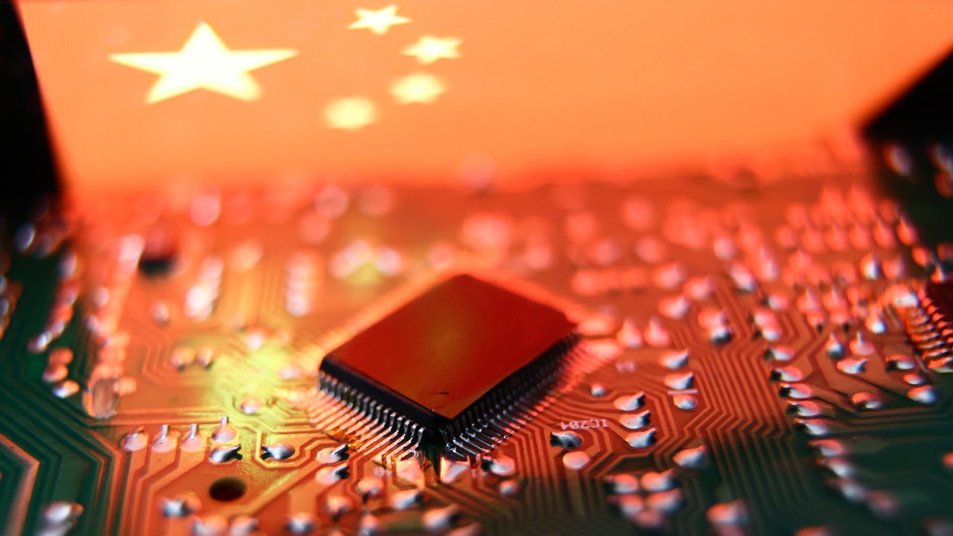
SMIC's 7nm beats Intel 18A on pitch, trails 38% on density
Key Takeaways
- SMIC's N+3 process achieves 32.5nm metal pitch without EUV, beating Intel 18A's 36nm shipping pitch
- Despite the tighter pitch, SMIC trails Intel 18A by 38% in overall transistor density
- The Kirin 9030's prime core performance matches 2021-era Android flagships, not current competitors
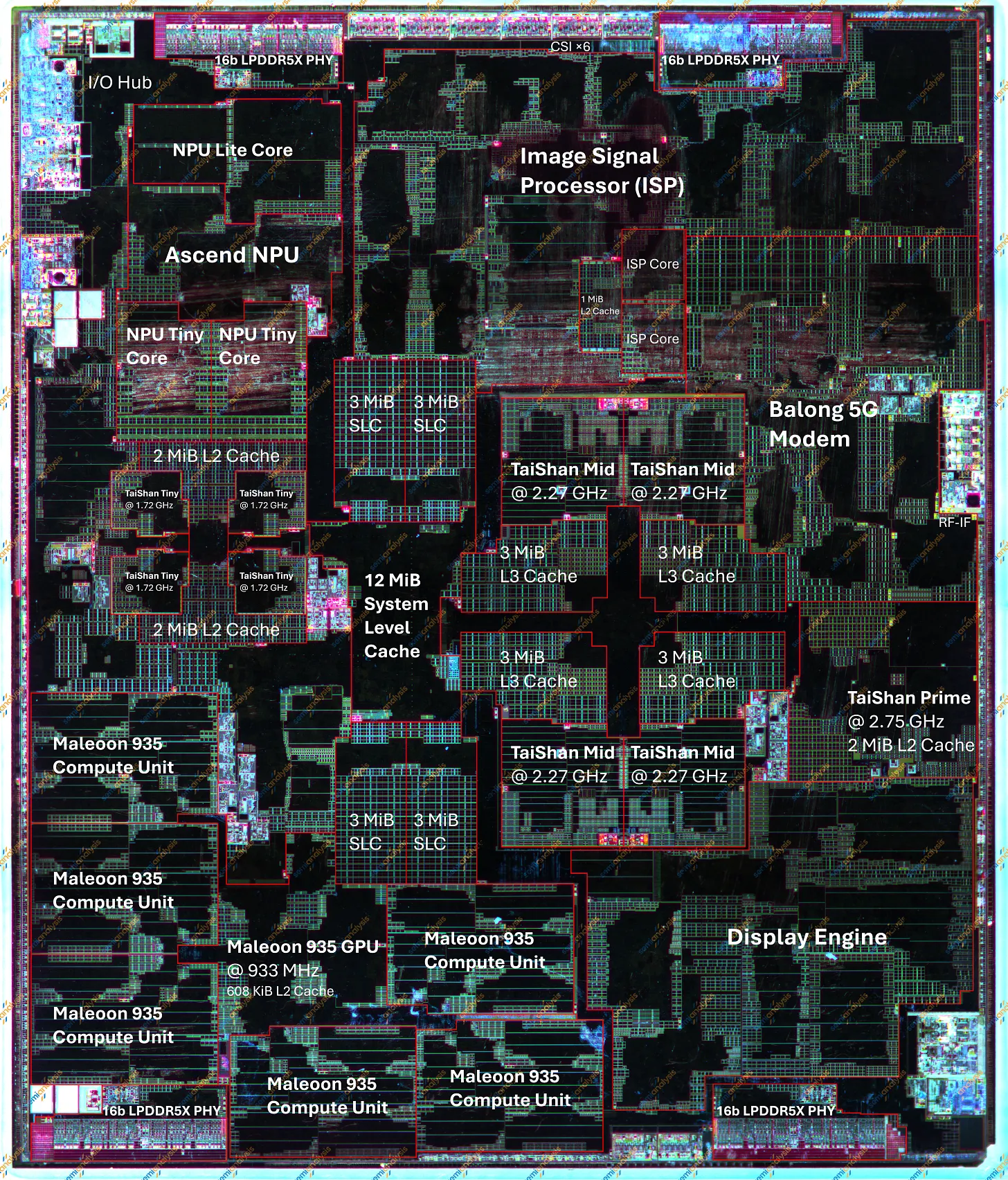
SMIC's third-generation 7nm process achieves a 32.5nm minimum local metal pitch, tighter than the 36nm pitch Intel ships in its Panther Lake processors on 18A. The catch: SMIC still trails Intel's overall transistor density by 38%. SemiAnalysis published these findings from its new in-house teardown lab, analyzing the HiSilicon Kirin 9030 inside Huawei's Mate 80 phones.
The headline number sounds like a win for China's leading foundry. It isn't. Metal pitch is one metric among many, and SMIC paid dearly for that 32.5nm figure. The company achieved it without EUV lithography, relying instead on DUV tools and quadruple-patterning that demands extra masking and etch passes. Every workaround adds complexity and cost.
Why does Intel still lead despite the wider pitch?
Intel's 18A process supports a 32nm minimum metal pitch, but Panther Lake ships at a relaxed 36nm. The company chose this deliberately. PowerVia, Intel's backside power delivery technology, routes power through the back of the wafer. This clears the front-side metal stack for signal wiring, buying roughly 10% higher density and allowing looser front-side pitches without sacrificing overall performance.
The result: a node built on GAA RibbonFET transistors and backside power can ship a wider local pitch than a DUV Chinese process and still maintain a wide overall lead. SMIC's N+3 hits 113.4 million transistors per square millimeter. That puts it just ahead of TSMC's mature N6 node at 107.7 million, but well behind Intel 18A. In relative terms, SMIC delivers only 62% of Intel's density.
What tricks did SMIC use to hit 32.5nm?
Without access to ASML's EUV machines, SMIC deployed every density trick available. The N+3 process uses two fins per transistor, lands contacts directly over the active gate, and implements single diffusion breaks between cells. Each technique squeezes out marginal gains at the cost of manufacturing complexity.
Quadruple-patterning, the core of SMIC's approach, multiplies the number of lithography steps required. More steps mean more potential defects, lower yields, and higher per-chip costs. Community discussions on Hacker News note this is likely unsustainable compared to Intel's PowerVia-enabled process, which achieves better results with fewer manufacturing headaches.
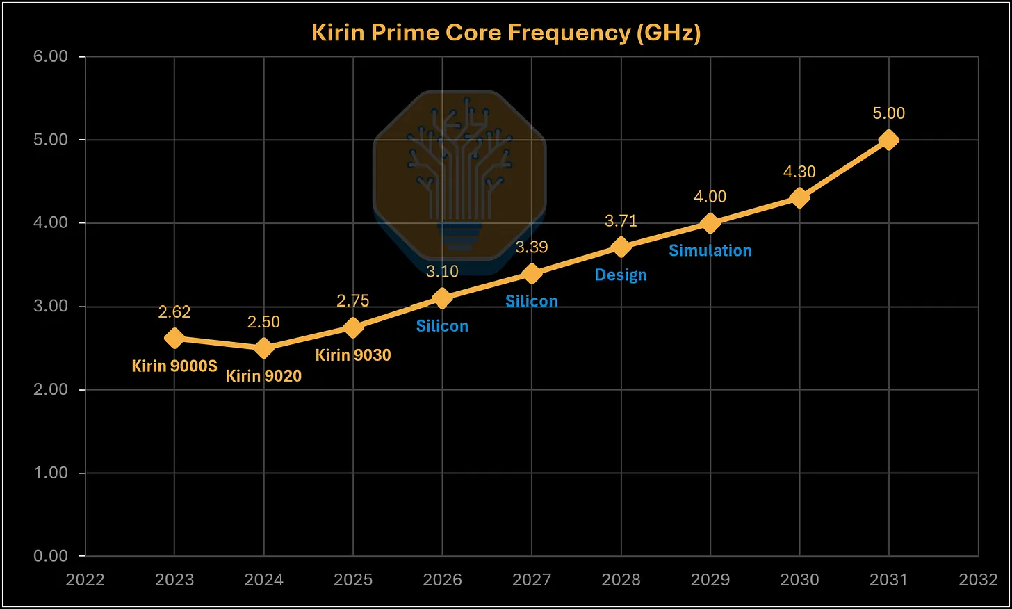
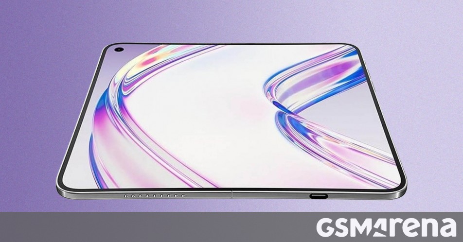
Kirin 9030 performance lags three years behind
The Kirin 9030 Pro's prime core runs at 2.75 GHz and delivers per-clock performance near Arm's 2021-era Cortex-X2. That leaves it roughly level with Android flagships from three years ago. Current processors from Apple, Qualcomm, MediaTek, and Samsung all outpace it.
Huawei's roadmap targets 5 GHz by 2031. SemiAnalysis notes that goal is "far beyond what planar scaling alone could deliver." Reaching that frequency would require either access to more advanced lithography or fundamental architectural changes that current sanctions block.
SemiAnalysis opens teardown lab to challenge TechInsights
The Kirin 9030 analysis marks the first public output from SemiAnalysis's new Teardown Engineering & Evaluation Lab (STEEL) in Hillsboro, Oregon. The company spent 18 months building the facility and has already generated revenue analyzing datacenter silicon, including TSMC customer chiplets with advanced 3D stacking.
SemiAnalysis is positioning itself against TechInsights, the Ottawa-based firm that has dominated semiconductor reverse engineering for years. TechInsights is backed by private equity, including Oakley Capital and CVC Growth. SemiAnalysis claims its rival is up for sale and has underinvested in equipment, though TechInsights hasn't confirmed either point.
The teardown also found the Kirin 9030 Pro carrying Samsung LPDDR5X memory. Some 16 GB variants use DRAM from Chinese maker CXMT, indicating Huawei is diversifying its supply chain where possible.
What this means for SMIC and Huawei
SMIC can produce chips that compete on narrow metrics. But narrow metrics don't ship competitive products. The 38% density gap translates directly to larger dies, higher power consumption, and worse thermal performance for any given design. Huawei's Mate 80 phones work, but they're built on technology that trails the industry by years.
The sanctions imposed on Chinese semiconductor companies aimed to slow their progress. This teardown suggests they're working. SMIC is burning engineering effort and manufacturing complexity to achieve results that Western foundries accomplish more elegantly. That's survivable in the short term but increasingly costly as the gap widens.
Logicity's Take
SMIC's tighter metal pitch is impressive engineering, but it's the semiconductor equivalent of winning a drag race by removing the doors. The company is trading manufacturing efficiency and yield for density gains that still don't close the gap. Unless export controls ease, Huawei will continue shipping phones that feel like time machines to 2021.
Frequently Asked Questions
What is metal pitch in semiconductor manufacturing?
Metal pitch is the center-to-center distance between adjacent metal wires on a chip. Smaller pitch allows more transistors per area, but requires more precise lithography.
Why can't SMIC use EUV lithography?
U.S. and allied export controls prevent ASML from selling EUV machines to Chinese companies. SMIC must rely on older DUV tools with multi-patterning techniques.
How does Intel's PowerVia affect chip density?
PowerVia routes power through the back of the chip, freeing front-side metal layers for signal routing. This allows Intel to achieve higher density even with wider metal pitches.
Is the Kirin 9030 competitive with current flagship processors?
No. Its prime core performance matches 2021-era chips, leaving it behind current offerings from Apple, Qualcomm, MediaTek, and Samsung.
What is SemiAnalysis's STEEL lab?
The Teardown Engineering & Evaluation Lab in Hillsboro, Oregon, is SemiAnalysis's new facility for reverse-engineering advanced semiconductors, competing with TechInsights.
Understanding how hardware limitations affect performance tradeoffs
Need Help Implementing This?
Logicity helps businesses understand semiconductor supply chain implications. Contact us for briefings on how chip manufacturing trends affect your hardware roadmap.
Source: Latest from Tom's Hardware
Huma Shazia
Senior AI & Tech Writer
Related Articles
Browse all
Alienware AW2726DM Review: The $350 QD-OLED Gaming Monitor That Changes Everything
Dell's Alienware AW2726DM shatters the OLED gaming monitor price barrier at just $350, delivering 27-inch QHD resolution, 240Hz refresh rate, and Quantum Dot color that rivals monitors costing twice as much. This isn't an incremental price drop. It's a complete reset of what budget-conscious gamers can expect.
iPhone Fold Launch 2026: Apple's First Foldable Could Capture 19% Market Share Instantly
Apple's long-awaited foldable iPhone is finally coming, and analysts predict it'll rocket the company to third place in the foldable market behind Samsung and Huawei. The secret weapon? Some seriously clever material science that could solve the crease problem that's plagued every foldable phone so far.

FAA Approves Military Laser Weapons for Drone Defense: What the New Airspace Rules Mean for Border Security
The FAA has given the Pentagon full approval to use high-energy laser systems against drones in US airspace, ending a two-month standoff that started when lasers shot down party balloons mistaken for cartel drones. The decision comes after safety assessments concluded these weapons don't pose increased risk to civilian aircraft.
China Chip Subsidies Reach $142 Billion: 3.6x More Than US Spent on Semiconductor Manufacturing
A new CSIS report reveals China has poured $142 billion into semiconductor subsidies over the past decade, dwarfing US spending by a factor of 3.6. But here's the twist: despite this massive investment, Chinese chipmakers still lag years behind TSMC and struggle with abysmal yields at advanced nodes.