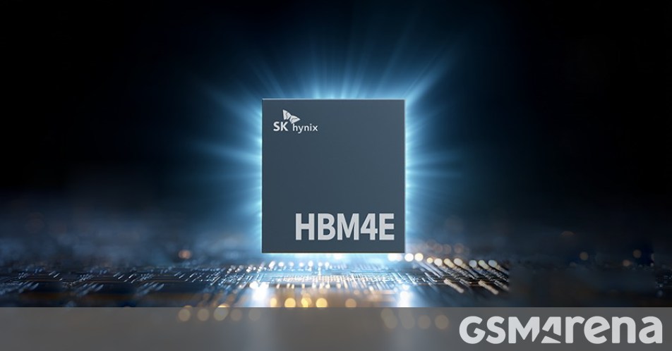
SK hynix ships HBM4E samples: 16Gbps, 48GB per stack
Key Takeaways
- SK hynix HBM4E delivers 16Gbps per pin, 60% faster than HBM4 and 14% faster than Samsung's competing design
- 12-layer stacks provide 48GB capacity with 20% better power efficiency than previous generation
- New MR-MUF construction reduces heat resistance by 17%, critical for densely packed AI data centers
SK hynix has started shipping samples of its HBM4E memory to customers, pushing per-pin bandwidth to 16Gbps. That figure beats Samsung's competing HBM4E design, which samples at 14Gbps, by roughly 14%. The Korean memory giant is staking its claim as the leader in AI accelerator memory at a moment when demand from NVIDIA, AMD, and hyperscalers shows no sign of slowing.
The samples feature 12 memory dies stacked vertically, yielding 48GB of capacity per stack. AI accelerators typically use multiple stacks, so a chip with six HBM4E stacks would carry 288GB of ultra-fast memory. For context, NVIDIA's current H100 uses 80GB of HBM3 across five stacks. The jump to HBM4E should allow next-generation chips to handle larger model weights without swapping data to slower system memory.
How does HBM4E compare to HBM4?
The leap from HBM4 to HBM4E is substantial. HBM4 topped out at 10Gbps per pin. HBM4E hits 16Gbps, a 60% increase in raw bandwidth. SK hynix also claims a 20% improvement in power efficiency, which matters enormously in data centers where cooling costs rival compute costs.
Beyond speed and efficiency, the physical construction changed. SK hynix uses a process called MR-MUF, short for Mass Reflow Molded Underfill. The technique fills gaps between stacked silicon dies with a protective liquid that hardens into a solid. The result: 17% lower thermal resistance than older designs. Heat dissipation is a genuine engineering challenge when you stack 12 chips on top of each other and run them at maximum bandwidth.
| Specification | HBM4 | SK hynix HBM4E | Samsung HBM4E |
|---|---|---|---|
| Bandwidth per pin | 10 Gbps | 16 Gbps | 14 Gbps |
| Stack height | 8-12 layers | 12 layers | 12 layers |
| Capacity per stack | Up to 36GB | 48GB | 48GB |
| Power efficiency vs HBM4 | Baseline | +20% | Not disclosed |
Why AI hardware needs HBM
Standard DDR memory, the kind in your laptop or server, connects to processors through traces on a motherboard. That physical distance creates latency. Bandwidth caps out around 50-60GB/s per channel. AI training and inference demand orders of magnitude more.
HBM solves this by stacking memory dies vertically and bonding them directly to the processor package via a silicon interposer. The connection is shorter, wider, and faster. A single HBM4E stack at 16Gbps across a 2048-bit interface delivers over 4TB/s of bandwidth. Multiply that by several stacks, and you get the memory throughput that makes training trillion-parameter models feasible.
SK hynix has dominated this market. The company reportedly supplies over 90% of NVIDIA's HBM needs. Samsung and Micron have struggled to match SK hynix's yields and specifications, though Samsung's recent 14Gbps HBM4E samples show the gap is narrowing.
When will HBM4E reach mass production?
SK hynix's press release states the company delivered samples "on schedule" and will "work closely with partners for mass production in a timely manner." That corporate phrasing translates to: volume production probably starts in late 2025 or early 2026, assuming validation goes smoothly.
Samsung began sampling its HBM4E about a month before SK hynix's announcement. The two companies are racing to win design slots in upcoming AI accelerators from NVIDIA, AMD, and custom silicon projects at Google, Amazon, and Microsoft. Winning those slots means billions in revenue.
The pricing and supply question
HBM is expensive. Manufacturing yields are lower than standard DRAM because stacking 12 dies with perfect alignment and connectivity is hard. Demand from AI infrastructure has outstripped supply for two years running. Analysts at TrendForce project the HBM market will exceed $20 billion by the end of 2025.
One consequence: memory makers have shifted fab capacity toward HBM and away from consumer DRAM. That reallocation contributed to tight supply and elevated prices for graphics cards and other consumer hardware throughout 2024. HBM4E's higher complexity could extend that dynamic.
Logicity's Take
SK hynix hitting 16Gbps while Samsung lags at 14Gbps matters more than the raw numbers suggest. NVIDIA and AMD design their next-generation chips around specific memory specs. If SK hynix can deliver higher bandwidth at volume, it locks in multi-year supply agreements before Samsung catches up. The 17% thermal improvement is equally strategic. Data center operators pay real money to cool racks. Any reduction in heat resistance translates directly to lower operating costs and denser deployments. SK hynix is selling efficiency as much as speed.
Frequently Asked Questions
What is HBM4E memory?
HBM4E is the latest generation of High Bandwidth Memory, designed for AI accelerators and GPUs. It stacks memory dies vertically and connects them directly to processors for bandwidth exceeding 4TB/s per stack.
How fast is SK hynix HBM4E?
SK hynix's HBM4E delivers 16Gbps per pin, 60% faster than HBM4 (10Gbps) and 14% faster than Samsung's competing 14Gbps HBM4E design.
When will HBM4E be available?
SK hynix is currently shipping samples to partners. Mass production is expected in late 2025 or early 2026, depending on validation timelines.
Why does AI hardware use HBM instead of DDR?
HBM provides 10-50x more bandwidth than DDR by stacking memory dies and connecting them directly to the processor. AI training requires this bandwidth to feed data to thousands of compute cores simultaneously.
How much capacity does HBM4E offer?
SK hynix's 12-layer HBM4E stacks provide 48GB each. AI accelerators using six stacks would have 288GB of high-bandwidth memory.
Need Help Implementing This?
Building AI infrastructure or evaluating memory options for your next hardware deployment? Logicity covers the technologies shaping enterprise computing. Subscribe for weekly analysis on semiconductors, cloud infrastructure, and developer tools.
Source: GSMArena.com / Peter
Manaal Khan
Tech & Innovation Writer
Related Articles
Browse all
Alienware AW2726DM Review: The $350 QD-OLED Gaming Monitor That Changes Everything
Dell's Alienware AW2726DM shatters the OLED gaming monitor price barrier at just $350, delivering 27-inch QHD resolution, 240Hz refresh rate, and Quantum Dot color that rivals monitors costing twice as much. This isn't an incremental price drop. It's a complete reset of what budget-conscious gamers can expect.

iPhone Fold Launch 2026: Apple's First Foldable Could Capture 19% Market Share Instantly
Apple's long-awaited foldable iPhone is finally coming, and analysts predict it'll rocket the company to third place in the foldable market behind Samsung and Huawei. The secret weapon? Some seriously clever material science that could solve the crease problem that's plagued every foldable phone so far.

FAA Approves Military Laser Weapons for Drone Defense: What the New Airspace Rules Mean for Border Security
The FAA has given the Pentagon full approval to use high-energy laser systems against drones in US airspace, ending a two-month standoff that started when lasers shot down party balloons mistaken for cartel drones. The decision comes after safety assessments concluded these weapons don't pose increased risk to civilian aircraft.

China Chip Subsidies Reach $142 Billion: 3.6x More Than US Spent on Semiconductor Manufacturing
A new CSIS report reveals China has poured $142 billion into semiconductor subsidies over the past decade, dwarfing US spending by a factor of 3.6. But here's the twist: despite this massive investment, Chinese chipmakers still lag years behind TSMC and struggle with abysmal yields at advanced nodes.