Key Takeaways
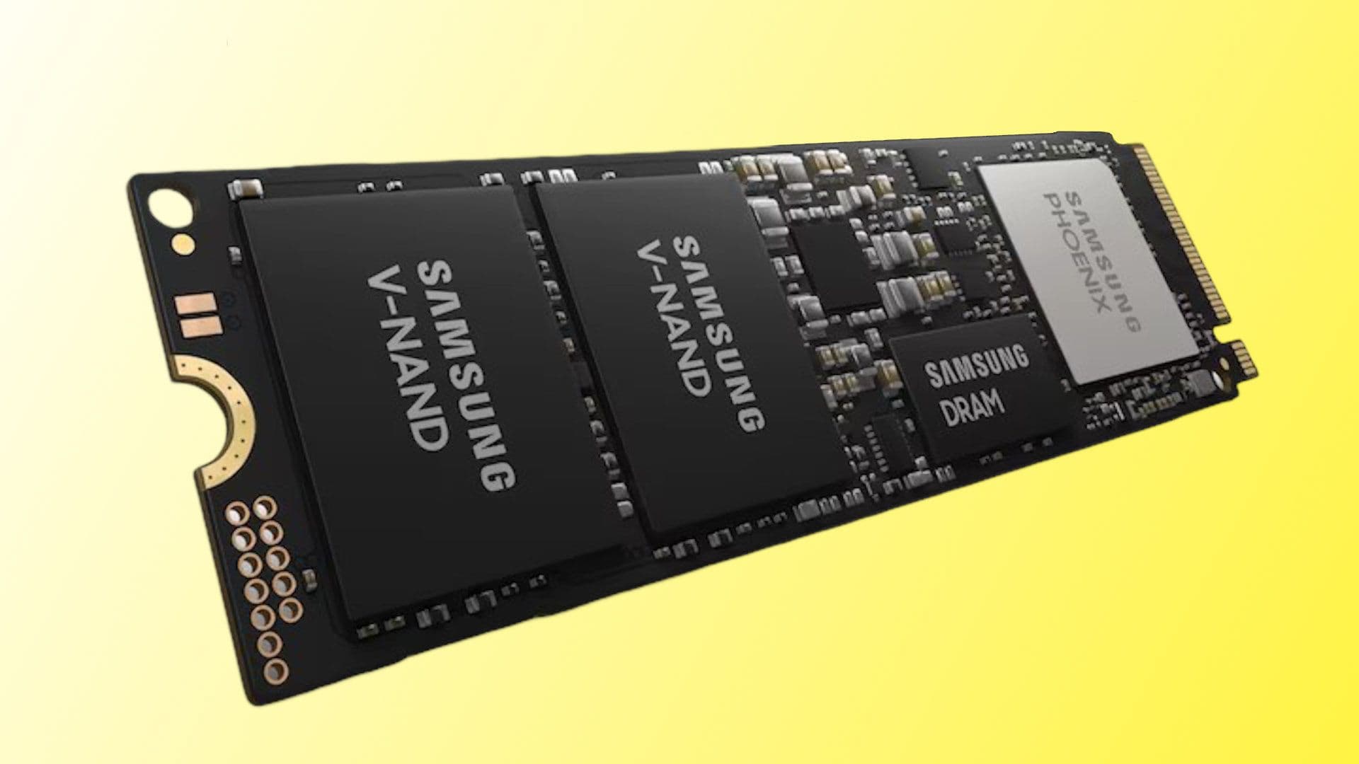
- Samsung achieved 900 layers by bonding two 450-layer wafers using Cell Multi-Bonding (CMB) technology
- The prototype offers roughly 3x the density of current NAND flash, with SK Hynix's 321-layer chips being the current leader
- Consumer SSD prices are unlikely to drop soon because AI infrastructure is absorbing all available flash capacity
Two Wafers, One Chip
Samsung has built a 900-layer NAND flash memory prototype, according to a report from ET News via Sammobile. The company didn't manufacture a single 900-layer tower. Instead, it bonded two separate 450-layer wafers into one integrated chip using what Samsung calls Cell Multi-Bonding (CMB) technology.
“Samsung Electronics recently implemented a 900-layer Class V-NAND integrated system utilizing Cell Multi-Bonding (CMB) technology, which bonds two 450-layer cell wafers into one.”
— ET News report
For context, SK Hynix currently holds the industry record with 321-layer NAND flash. Samsung's prototype represents nearly three times that density. The company is also preparing its 10th generation V-NAND with over 400 layers for mass production, expected in late 2026. The 900-layer prototype appears to bond two of those next-gen chips together.
The Engineering Challenge
Bonding two wafers sounds simple. It isn't. The process requires aligning cell wafers and their interconnects with extreme precision. A bigger problem is wafer warping during manufacture, which occurs when the thin silicon flexes under heat and pressure.
Samsung solved the warping issue with an advanced Upper Chuck design. The Upper Chuck is the tool that holds wafers in place during the bonding process. By improving how it grips and stabilizes the wafers, Samsung kept them flat enough to bond accurately.
This approach, called multi-bonding, represents a shift in how the industry thinks about NAND scaling. For years, manufacturers competed to stack more layers in a single monolithic tower. That approach is hitting physical limits around 300-400 layers. Bonding separate wafers together offers a workaround.
When Will SSDs Get Cheaper?
Here's the uncomfortable truth: probably not soon. Higher density normally means lower cost per gigabyte. But economics isn't cooperating.
AI infrastructure is consuming flash storage at a pace that exceeds supply growth. Data centers training and running large language models need massive amounts of fast storage. As long as hyperscalers and cloud providers will pay premium prices, consumer SSDs stay expensive.
A 2TB M.2 SSD currently costs around $250. That's not outrageous, but it's not cheap either. The technology exists to make storage much denser. The market doesn't yet have a reason to make it much cheaper.
Online discussions around this announcement reflect that skepticism. Users on r/hardware and Hacker News point out that enterprise AI storage demand is currently outpacing supply. Technical breakthroughs don't automatically translate to retail price drops when every new gigabyte already has a buyer.
Samsung's Roadmap to 1,000 Layers
Samsung has previously stated it aims to reach 1,000 layers by 2030. The 900-layer prototype suggests the company is on track. The path forward relies on multi-bonding rather than monolithic stacking.
The transition matters because it changes what's possible. Monolithic stacking faces diminishing returns. Each additional layer becomes harder to manufacture reliably. Multi-bonding sidesteps the problem by using proven wafer technology and focusing engineering effort on the bonding process itself.
If Samsung can reliably bond three or four wafers, the layer counts could keep climbing without reinventing the fundamental memory cell architecture.
Logicity's Take
What This Means for PC Storage
For now, nothing changes at the retail level. The technology is in prototype stage. Even when it reaches production, enterprise buyers will absorb initial capacity.
The optimistic scenario: AI investment cools, data center demand normalizes, and surplus flash floods the consumer market. We've seen this pattern before. Crypto mining once created GPU shortages. When crypto crashed, graphics cards became plentiful.
The pessimistic scenario: AI demand keeps growing, new capacity feeds new data centers, and consumer storage remains an afterthought. In that world, we get technically impressive SSDs at uninspiring prices.
Related memory technology advancement from Samsung's main competitor
Frequently Asked Questions
How did Samsung achieve 900 layers in a NAND chip?
Samsung bonded two 450-layer wafers together using Cell Multi-Bonding (CMB) technology rather than manufacturing a single 900-layer tower.
When will 900-layer NAND reach consumer SSDs?
Samsung hasn't announced production timelines for the 900-layer prototype. The company's 10th-gen V-NAND with 430+ layers is expected in late 2026, suggesting 900-layer products are several years away.
Will this make SSDs cheaper?
Not immediately. AI infrastructure demand is absorbing available flash capacity. Consumer prices are unlikely to drop significantly until enterprise demand stabilizes or manufacturing scales dramatically.
What is the current highest layer count in production NAND?
SK Hynix holds the current record with 321-layer NAND technology in production.
What is Samsung's target for NAND layer count?
Samsung has stated it aims to reach 1,000 layers by 2030.
Need Help Implementing This?
Source: PCGamer latest
Huma Shazia
Senior AI & Tech Writer
Produced with AI assistance and reviewed by the Logicity editorial team. Learn more in our Editorial Policy.