Key Takeaways

- Qualcomm's HBC architecture places AI accelerators directly beneath DRAM stacks using through-silicon vias, eliminating expensive HBM and silicon interposers
- The company claims 6x higher bandwidth-per-watt versus HBM and 200x the capacity of on-chip SRAM, though actual bandwidth figures remain undisclosed
- AI250 and AI350 accelerators will ship later this year, with the AI250 promising 18x the bandwidth of the current AI200
Qualcomm on Wednesday unveiled its HBC near-memory compute architecture, a design that places AI accelerators directly beneath LPDDR DRAM stacks rather than relying on expensive high-bandwidth memory. The company claims the approach delivers 6x higher bandwidth-per-watt than traditional HBM solutions and 200x the capacity of on-chip SRAM. If those numbers hold up in production, Qualcomm could have a genuine alternative to the HBM-based designs that currently dominate data center AI.
The "memory wall" is a familiar villain in AI compute. Processor speeds have outpaced memory bandwidth for decades, but the problem has become acute with transformer models that shuffle enormous tensors between memory and compute units. HBM helps, but it requires expensive silicon interposers and advanced packaging. Qualcomm's bet: skip HBM entirely by putting the accelerator under the memory.
How Qualcomm's HBC architecture works
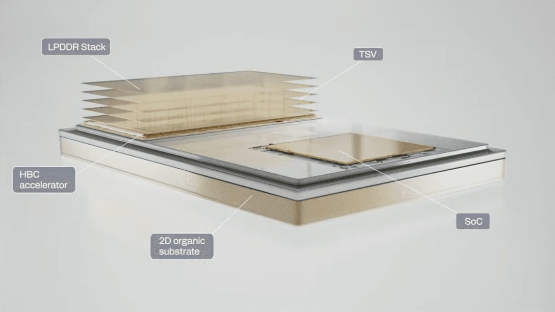
The design disaggregates the AI accelerator from the main system-on-chip and positions it directly beneath an LPDDR DRAM stack. Through-silicon vias connect the two, providing a wide, short data path without the silicon interposer that HBM solutions require. This matters because interposers are expensive to manufacture and add thermal complexity.
“We have separated the AI accelerator from the XPU and placed the XPU directly beneath a DRAM stack. This gives us the performance advantages of SRAM with the density and capacity of stacked memory. The congestion associated with HBM is gone.”
— Tony Pialis, Executive Vice President and General Manager of Data Center Business at Qualcomm
Pialis also highlighted the cost angle: lower power consumption, reduced heat, and the ability to deploy multiple HBC stacks within a single compute device using standard packaging. That last point is significant. If HBC works with conventional packaging, it avoids the supply chain bottlenecks that have plagued HBM production.
What Qualcomm isn't telling us
The announcement comes with notable gaps. Qualcomm has not disclosed absolute bandwidth numbers, which makes it difficult to compare HBC directly to HBM3E solutions or to competing near-memory approaches. The 6x bandwidth-per-watt claim is a relative metric, and the baseline matters.
More fundamentally, Qualcomm has not explained what the HBC accelerator actually does. Is it a transformer-specific inference engine? A general tensor processor? Preprocessing logic for larger systems? The company's silence on this point makes it hard to assess where HBC fits in a data center stack.
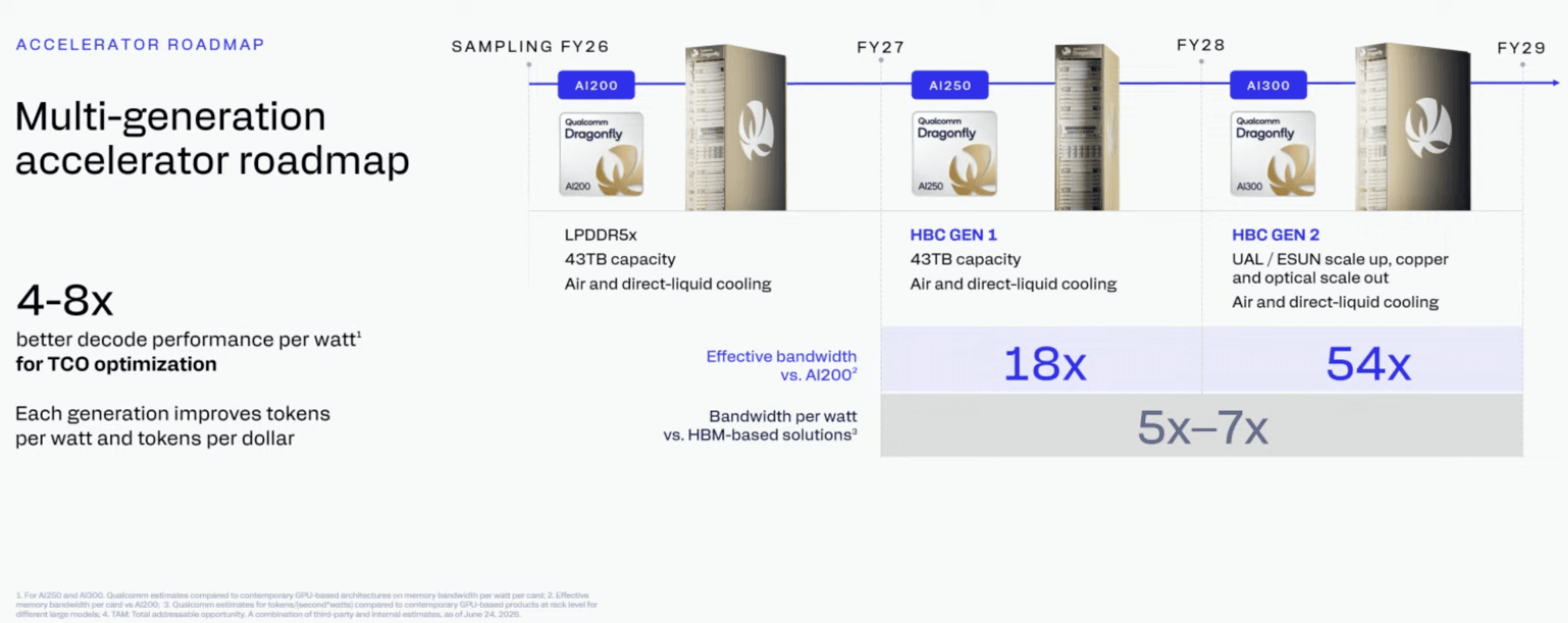
The AI200, AI250, and AI300 roadmap
Qualcomm also outlined its accelerator roadmap. The AI200, due later this year, uses LPDDR5X and offers 43 TB of RAM per rack. It's the current-generation product without HBC.
The AI250 will be the first product with first-generation HBC, claiming 18x the bandwidth of the AI200. The AI300 follows with second-generation HBC, promising 54x the bandwidth of the AI200. Qualcomm did not provide ship dates for the AI250 or AI300.
Near-memory compute isn't new, but adoption has been slow
Putting DRAM on or near logic has been an industry aspiration for years. Every major DRAM maker has experimented with the approach. None have achieved widespread adoption. The challenge isn't just technical. It requires coordinating memory vendors, foundries, and system designers around a new architecture.
GUC, a fabless ASIC design service company, recently proposed a DRAM-on-Logic (DoL) technology that stacks one to four DRAM layers on top of logic, claiming around 5 TB/s of bandwidth. GUC says this beats some HBM3E subsystems without advanced packaging. Qualcomm's HBC sounds conceptually similar, but without bandwidth numbers, direct comparison is impossible.
Why this matters for data center AI
The data center AI accelerator market is dominated by NVIDIA's GPUs, with AMD's MI300 series and Intel's Gaudi chips as distant competitors. All three rely on HBM. If Qualcomm can deliver competitive performance without HBM, it could undercut rivals on cost and power, both critical factors for hyperscalers optimizing inference at scale.
But the "if" is doing a lot of work in that sentence. Qualcomm has announced an architecture, not a shipping product with published benchmarks. The AI250 with first-generation HBC doesn't have a public ship date. Until customers can run real workloads, the claims remain claims.
Logicity's Take
Qualcomm's HBC architecture addresses a real bottleneck, but the announcement raises more questions than it answers. The refusal to disclose absolute bandwidth or explain what the accelerator actually computes suggests the technology is earlier-stage than the marketing implies. Hyperscalers will want to see MLPerf numbers, not efficiency ratios. Still, if Qualcomm can deliver 18x bandwidth improvements with standard packaging, it would represent a genuine cost advantage over HBM-based competitors. Watch for benchmark disclosures in the next two quarters.
Frequently Asked Questions
What is Qualcomm's HBC architecture?
HBC (High-Bandwidth Compute) is Qualcomm's near-memory AI architecture that places accelerators directly beneath LPDDR DRAM stacks using through-silicon vias, eliminating the need for expensive HBM memory and silicon interposers.
How does HBC compare to HBM in efficiency?
Qualcomm claims HBC delivers 6x higher bandwidth-per-watt compared to HBM and 200x the capacity of on-chip SRAM. However, the company has not disclosed absolute bandwidth figures.
When will Qualcomm's HBC-based accelerators ship?
The AI200 (using LPDDR5X, not HBC) is due later this year. The AI250 with first-generation HBC and AI300 with second-generation HBC are on the roadmap, but Qualcomm has not announced specific dates.
What is the memory wall problem in AI?
The memory wall refers to the growing gap between processor speeds and memory bandwidth. In AI workloads, this bottleneck limits performance because large models require moving massive amounts of data between memory and compute units.
Need Help Implementing This?
If your organization is evaluating AI accelerator options for inference workloads, reach out to Logicity's consulting team for vendor-neutral guidance on architecture selection, total cost of ownership analysis, and deployment planning.
Source: Latest from Tom's Hardware
Manaal Khan
Tech & Innovation Writer
Produced with AI assistance and reviewed by the Logicity editorial team. Learn more in our Editorial Policy.