Intel 18A-P enters risk production with 9% speed boost
Key Takeaways
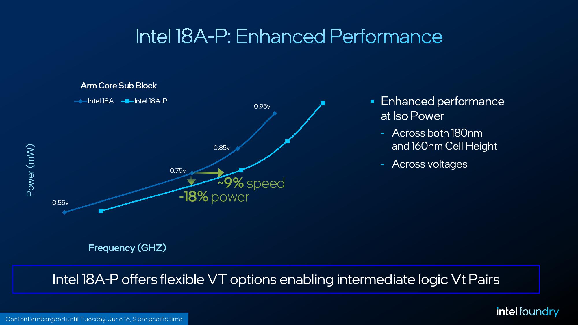
- Intel 18A-P delivers 9% higher frequency at the same power or 18% lower power at the same speed
- The node is backward compatible with existing 18A designs, requiring no redesign for customers
- New W3P transistor with dual contacts enables the biggest performance gains through Power Boost
Intel's 18A-P process node has entered risk production, the company revealed at VLSI 2026. The performance-optimized variant of Intel's 18A node promises a 9% frequency boost at the same power draw, or an 18% reduction in power consumption at matched performance levels. Products like Panther Lake and Xeon 6+ will use the original 18A, but 18A-P opens a faster path for designs that need extra headroom.

Risk production sits one step before high-volume manufacturing. Intel will produce full wafers on standard production lines, but at limited scale. The goal is to gather data on defect rates, performance consistency, and process variability before ramping up. For entirely new nodes, this phase typically runs 12 to 24 months ahead of mass production. Because 18A-P builds on an existing node rather than starting fresh, Intel expects a tighter timeline.
What makes 18A-P a drop-in upgrade?
The revision uses the same cell libraries as 18A. High Performance designs sit at 180mm cell height; High Density at 160mm. Any chip designed for 18A can move to 18A-P without modification. Designers will see modest performance gains even without touching their layouts.
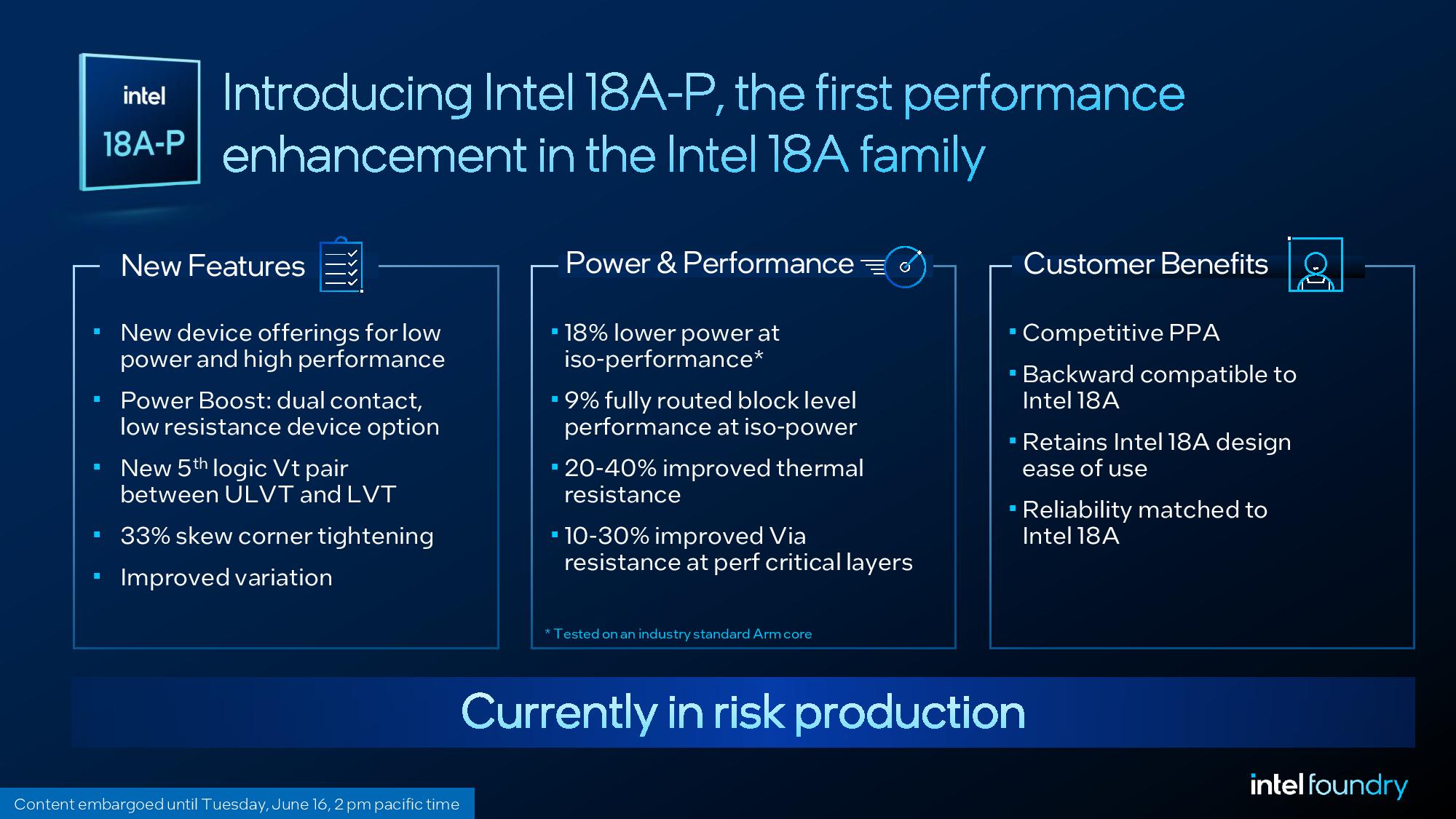
Intel tested its numbers on a standard Arm core subblock, measuring the 9% frequency gain and 18% power reduction specifically at 0.75 volts. The improvement holds across other voltage points, though the magnitude shifts. This matters because mobile and server chips operate across a range of voltages depending on workload.
Three new transistor designs expand the toolkit
Intel is adding W1, W1.5, and W3P to its transistor library. W1 was previously available only in the 160mm library; it now works in 180mm as well. W1.5 slots into 160mm. Both are narrow designs built for low-power applications, filling gaps in energy-optimized chip layouts.
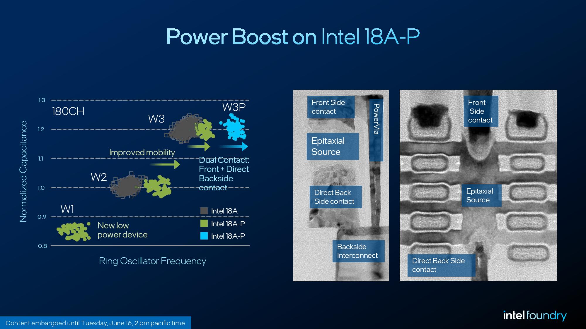
W3P is the standout. It's a dual-contact transistor that Intel calls "Power Boost." The 18A node already uses PowerVia, routing power through the back of the wafer to free up front-side space for signal wiring. W3P takes this further by placing contacts on both the front and back of the transistor. This cuts parasitic resistance and pushes higher drive current to the gate, speeding up switching times.
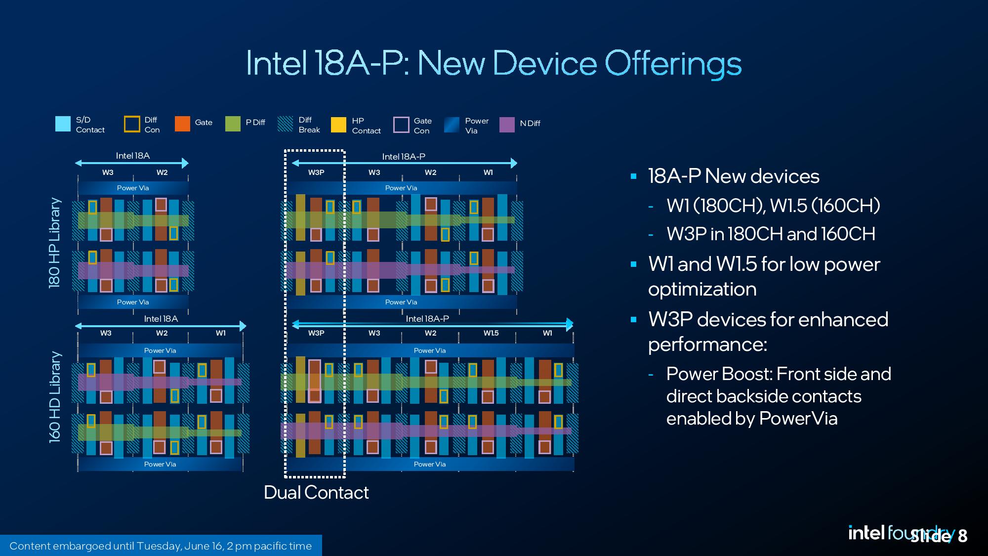
The original W2 and W3 transistors still benefit from the 18A-P process, but the gains are smaller. W3P delivers the biggest frequency jump, while W1 pushes designs into lower capacitance territory for battery-sensitive applications.
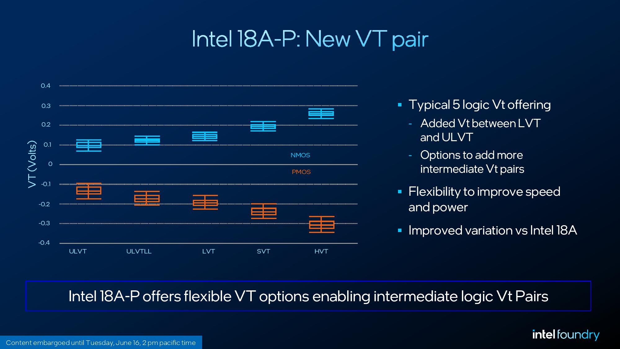
A new voltage threshold option for chip designers
Chip designers balance four standard threshold voltage (VT) options: HVT, SVT, LVT, and ULVT. Lower threshold voltages mean faster switching but higher leakage current. ULVT transistors perform best but waste the most power when idle. HVT transistors leak least but switch slowest.
Intel is adding ULVTLL, short for Ultra-Low Voltage Threshold Low Leakage. It sits between ULVT and LVT, giving designers a middle ground: better performance than LVT without the leakage penalty of ULVT. For chips that need to hit specific power targets while maximizing speed in certain blocks, this extra option could simplify tradeoffs.
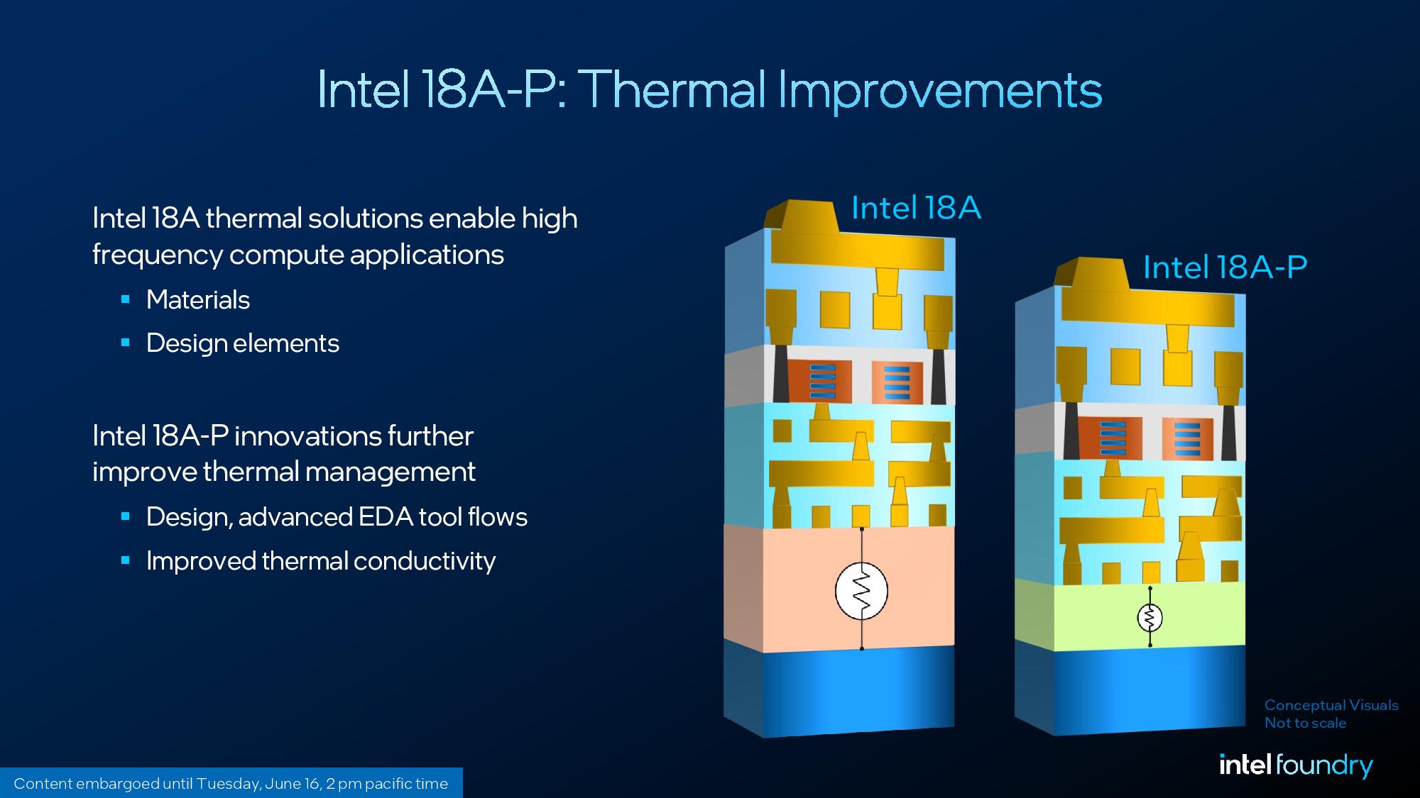
Thermal improvements target mobile and server chips
Intel claims 18A-P cuts thermal resistance by 20% to 40% through advanced wafer-thinning techniques. Lower thermal resistance means heat moves out of the chip faster, which matters for both thin laptops and densely packed server racks. The company also reports a 10x reduction in dynamic voltage droop, a refinement tied to PowerVia's backside power delivery.
Voltage droop occurs when sudden current spikes cause temporary voltage drops across the power delivery network. Excessive droop forces designers to add voltage guardbands, wasting power. A 10x improvement here could let chips run closer to their minimum operating voltage, squeezing out additional efficiency.
Where 18A-P fits in Intel's roadmap
Intel's "five nodes in four years" strategy aimed to regain process leadership after years of delays. The base 18A node is already in production for Panther Lake and Xeon 6+. 18A-P gives Intel a mid-generation refresh without forcing customers to redesign their chips. For foundry customers evaluating Intel Foundry Services against TSMC and Samsung, backward compatibility matters. Porting to a new process typically costs tens of millions of dollars and months of engineering time.
Community reaction has focused on what this means for Intel's competitiveness. On HackerNews, discussions centered on whether Intel's defect density and yield ramp can match TSMC's leading-edge nodes. Reddit's r/intel community emphasized the thermal improvements, noting their potential impact on thin-and-light laptops where heat dissipation limits sustained performance.
Logicity's Take
The real story isn't the 9% speed bump. It's that Intel can offer a meaningful mid-cycle upgrade without breaking customer designs. TSMC has done this with N-series optimizations for years, and Intel matching that cadence signals its foundry operations are maturing. The thermal and voltage droop numbers, if they hold at scale, address two pain points that have historically pushed mobile OEMs toward TSMC. Whether Intel can convert this into actual foundry wins depends on yield, which we won't know until 18A-P ships in volume.
Frequently Asked Questions
When will Intel 18A-P reach mass production?
Intel hasn't announced a specific date, but risk production typically precedes mass production by 12 to 24 months. Because 18A-P builds on the existing 18A node, the timeline is expected to be shorter.
Can existing 18A chip designs use 18A-P without changes?
Yes. Intel designed 18A-P to be backward compatible with 18A. Chips designed for the original node can be manufactured on 18A-P with performance gains and no required design modifications.
What is PowerVia in Intel 18A?
PowerVia is Intel's backside power delivery technology. It routes power through the back of the wafer instead of the front, freeing up space for signal wiring and reducing thermal resistance.
How does 18A-P compare to TSMC's latest nodes?
Direct comparisons are difficult because manufacturers measure differently. Intel claims 18A competes with TSMC N2 in density and performance. 18A-P adds incremental improvements that could strengthen Intel's position.
Which Intel products will use 18A-P?
Intel hasn't announced specific products for 18A-P yet. Panther Lake and Xeon 6+ use the base 18A node. Future product generations or refreshes could adopt 18A-P.
Another look at how chip performance shapes consumer hardware
Need Help Implementing This?
If you're evaluating foundry options for your next chip design or need guidance on process node selection, Logicity can connect you with semiconductor consulting experts. Contact our team for introductions to specialists in chip design and manufacturing strategy.
Source: Latest from Tom's Hardware
Huma Shazia
Senior AI & Tech Writer
Related Articles
Browse all
Alienware AW2726DM Review: The $350 QD-OLED Gaming Monitor That Changes Everything
Dell's Alienware AW2726DM shatters the OLED gaming monitor price barrier at just $350, delivering 27-inch QHD resolution, 240Hz refresh rate, and Quantum Dot color that rivals monitors costing twice as much. This isn't an incremental price drop. It's a complete reset of what budget-conscious gamers can expect.

iPhone Fold Launch 2026: Apple's First Foldable Could Capture 19% Market Share Instantly
Apple's long-awaited foldable iPhone is finally coming, and analysts predict it'll rocket the company to third place in the foldable market behind Samsung and Huawei. The secret weapon? Some seriously clever material science that could solve the crease problem that's plagued every foldable phone so far.

FAA Approves Military Laser Weapons for Drone Defense: What the New Airspace Rules Mean for Border Security
The FAA has given the Pentagon full approval to use high-energy laser systems against drones in US airspace, ending a two-month standoff that started when lasers shot down party balloons mistaken for cartel drones. The decision comes after safety assessments concluded these weapons don't pose increased risk to civilian aircraft.

China Chip Subsidies Reach $142 Billion: 3.6x More Than US Spent on Semiconductor Manufacturing
A new CSIS report reveals China has poured $142 billion into semiconductor subsidies over the past decade, dwarfing US spending by a factor of 3.6. But here's the twist: despite this massive investment, Chinese chipmakers still lag years behind TSMC and struggle with abysmal yields at advanced nodes.