imec, ASML, TSMC build 2D transistors at 50nm pitch
Key Takeaways
- imec, ASML, and TSMC achieved 50nm contacted poly pitch for 2D transistors, tighter than Intel's 10nm-class node
- 94% of transistors switched correctly with on/off ratios above 100,000, demonstrating production-viable yields
- The breakthrough uses standard 300mm wafers and single EUV exposure, no exotic tooling required
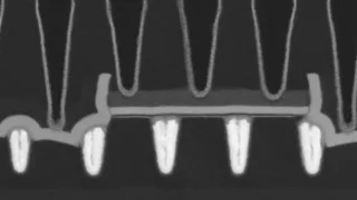
imec, ASML, and TSMC have fabricated complementary 2D-material transistors at 50nm contacted poly pitch on a standard 300mm wafer. That's tighter than Intel's 54nm pitch on its 10nm-class node. The consortium reported 94% of the integrated transistors switched correctly, with on/off current ratios above 100,000.
The results, presented this week at the IEEE/JSAP Symposium on VLSI Technology and Circuits, mark the first time both n-type and p-type 2D transistors have been integrated at this density on production-scale equipment. A single EUV lithography exposure printed channel lengths as short as 28nm.
Why 2D materials matter for post-silicon chips
Silicon transistors face fundamental physics problems as they shrink below 3nm. Electrons tunnel between channels at these scales, wasting power and degrading switching performance. 2D materials offer a path around this wall.
The n-channel devices in this demonstration use molybdenum disulfide (MoS₂), while p-channel devices use tungsten diselenide (WSe₂) or tungsten disulfide (WS₂). These transition metal dichalcogenides form layers less than a nanometer thick. At that thickness, the gate electrode can control the channel far more precisely than it can control a silicon nanosheet several nanometers thick.
Researchers have studied these materials for over a decade. imec has fabricated MoS₂ test transistors since the late 2010s. The difference now: both transistor polarities built together on a standard process flow, not isolated devices patterned with coarser lithography.
How they solved the contact resistance problem
Contact resistance has blocked 2D transistor scaling for years. An atomically thin channel carries little current, and the junction between metal contacts and the 2D film throttles whatever current the channel can deliver. The metal pins the semiconductor's Fermi level and raises the Schottky barrier that charge carriers must cross.
Lab devices compensated by using large contact areas. That killed the pitch scaling that made 2D transistors worth pursuing in the first place.
The consortium broke this trade-off by building the transistor upside down. Instead of depositing metal onto the fragile 2D film after the channel is in place, they patterned tungsten-filled contact trenches first. Then they transferred the 2D channel on top, with the gate deposited over it.
imec calls this a "reverse" thin-film-transistor flow. The bottom-contact geometry produced clean off-state behavior, with both polarities stopping conduction at zero gate voltage.
“For the first time, we achieved 50nm CPP — a metric determined by both the gate length and source/drain contact length — without affecting the performance of the 2D n and pFETs.”
— Gouri Sankar Kar, VP of R&D for compute and memory device technologies at imec
Standard EUV tooling, no exotic equipment
The 28nm channels and 50nm pitch required only one EUV exposure. Standard 0.33-NA EUV scanners handled it. This matters because ASML's High-NA EUV systems, which target far tighter pitches, cost significantly more and remain in limited supply.
ASML credited EUV resolution for shrinking 2D channel lengths that earlier 300mm demonstrations had left large because they relied on older lithography tools.
The demonstrated transistors reached active widths down to 75nm and an equivalent oxide thickness near 2nm. imec reported the WSe₂ p-channel devices performed close to the best lab-scale results published so far, narrowing the gap on the historically weaker p-type side of 2D CMOS.
Where this sits on the roadmap
imec isn't alone in 2D research. Intel runs its own 300mm 2D-material program with imec. Samsung has demonstrated wafer-scale growth of single-crystal MoS₂. University groups have pushed monolayer MoS₂ transistors to gate pitches near the 1nm node.
What sets this work apart is the combination: complementary n- and p-type integration, EUV single-patterning, and a node-relevant pitch on full 300mm tooling, all at once.
On most industry roadmaps, 2D channels come after the complementary FET (CFET) architecture. imec's long-range plans place CFETs around 2033 and 2D-semiconductor channels closer to 2041. The IRDS industry roadmap pencils in 2D channels as early as 2034 at the 0.7nm node.
That timeline sits well beyond current production. But the 94% yield and production-compatible process demonstrated here suggest 2D transistors have crossed from academic curiosity to serious engineering program.
Frequently Asked Questions
What are 2D transistors?
Transistors using atomically thin channel materials like molybdenum disulfide (MoS₂) instead of silicon. These materials are less than a nanometer thick, allowing better gate control at extremely small scales.
Why can't silicon transistors keep shrinking?
Below 3nm, quantum tunneling causes electrons to leak between channels. This wastes power and degrades switching performance. 2D materials offer better electrostatic control at these scales.
When will 2D transistors appear in commercial chips?
Industry roadmaps place 2D-semiconductor channels around 2034-2041. imec expects them to follow complementary FET (CFET) architectures, which are projected for approximately 2033.
What makes this demonstration different from previous 2D transistor research?
It combines complementary n-type and p-type devices, EUV single-patterning, and production-relevant 50nm pitch on standard 300mm wafers. Previous work achieved these separately but not together.
Does this require ASML's expensive High-NA EUV machines?
No. The 50nm pitch was achieved with standard 0.33-NA EUV scanners using a single exposure. High-NA equipment targets tighter pitches.
Logicity's Take
The 94% yield figure is the real news here. Lab demonstrations of 2D transistors have existed for years, but most used hand-crafted devices that couldn't scale to manufacturing. Running both polarities through a standard 300mm flow with single-exposure EUV means the integration challenges are tractable, not theoretical. The 2034-2041 timeline still looks aggressive given how much work remains on contact resistance, doping uniformity, and defect density. But this moves 2D channels from "promising research direction" to "active development program."
Need Help Implementing This?
Logicity covers the semiconductor industry for technical leaders making infrastructure and investment decisions. Subscribe to our newsletter for weekly analysis of manufacturing breakthroughs and their business implications.
Source: Latest from Tom's Hardware
Manaal Khan
Tech & Innovation Writer
Related Articles
Browse all
Alienware AW2726DM Review: The $350 QD-OLED Gaming Monitor That Changes Everything
Dell's Alienware AW2726DM shatters the OLED gaming monitor price barrier at just $350, delivering 27-inch QHD resolution, 240Hz refresh rate, and Quantum Dot color that rivals monitors costing twice as much. This isn't an incremental price drop. It's a complete reset of what budget-conscious gamers can expect.

iPhone Fold Launch 2026: Apple's First Foldable Could Capture 19% Market Share Instantly
Apple's long-awaited foldable iPhone is finally coming, and analysts predict it'll rocket the company to third place in the foldable market behind Samsung and Huawei. The secret weapon? Some seriously clever material science that could solve the crease problem that's plagued every foldable phone so far.

FAA Approves Military Laser Weapons for Drone Defense: What the New Airspace Rules Mean for Border Security
The FAA has given the Pentagon full approval to use high-energy laser systems against drones in US airspace, ending a two-month standoff that started when lasers shot down party balloons mistaken for cartel drones. The decision comes after safety assessments concluded these weapons don't pose increased risk to civilian aircraft.

China Chip Subsidies Reach $142 Billion: 3.6x More Than US Spent on Semiconductor Manufacturing
A new CSIS report reveals China has poured $142 billion into semiconductor subsidies over the past decade, dwarfing US spending by a factor of 3.6. But here's the twist: despite this massive investment, Chinese chipmakers still lag years behind TSMC and struggle with abysmal yields at advanced nodes.