Key Takeaways
- IBM's nanostack architecture stacks transistors in two vertical layers, doubling density to 100 billion transistors per chip
- The design delivers up to 50% more performance and 70% better energy efficiency compared to IBM's previous 2nm technology
- Industry analysts say this approach could extend Moore's Law by 10-15 years
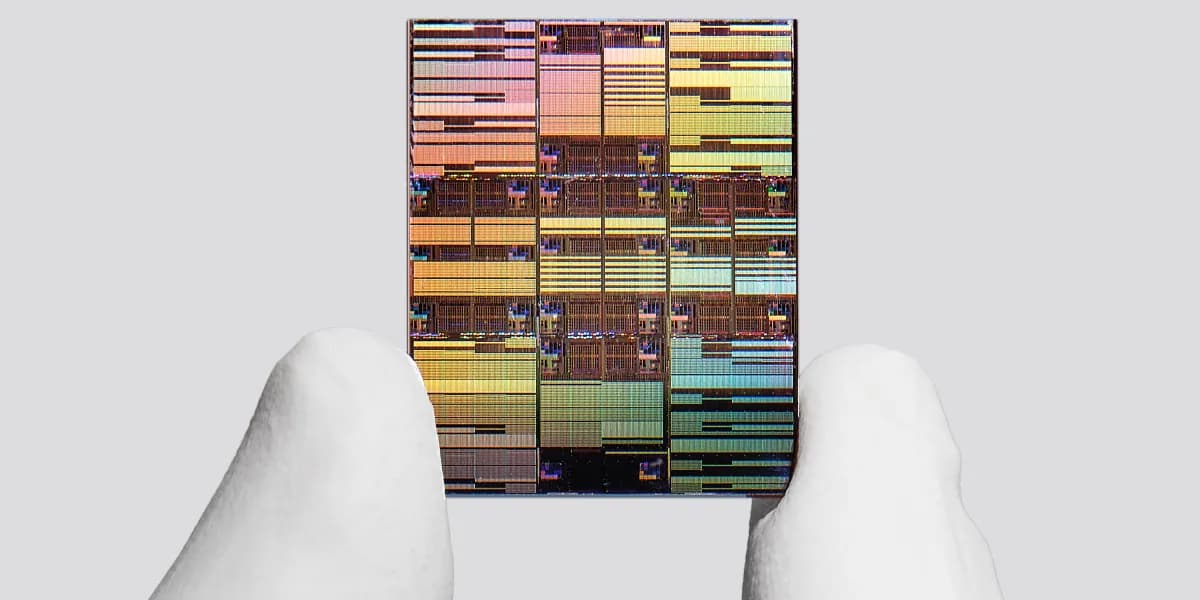
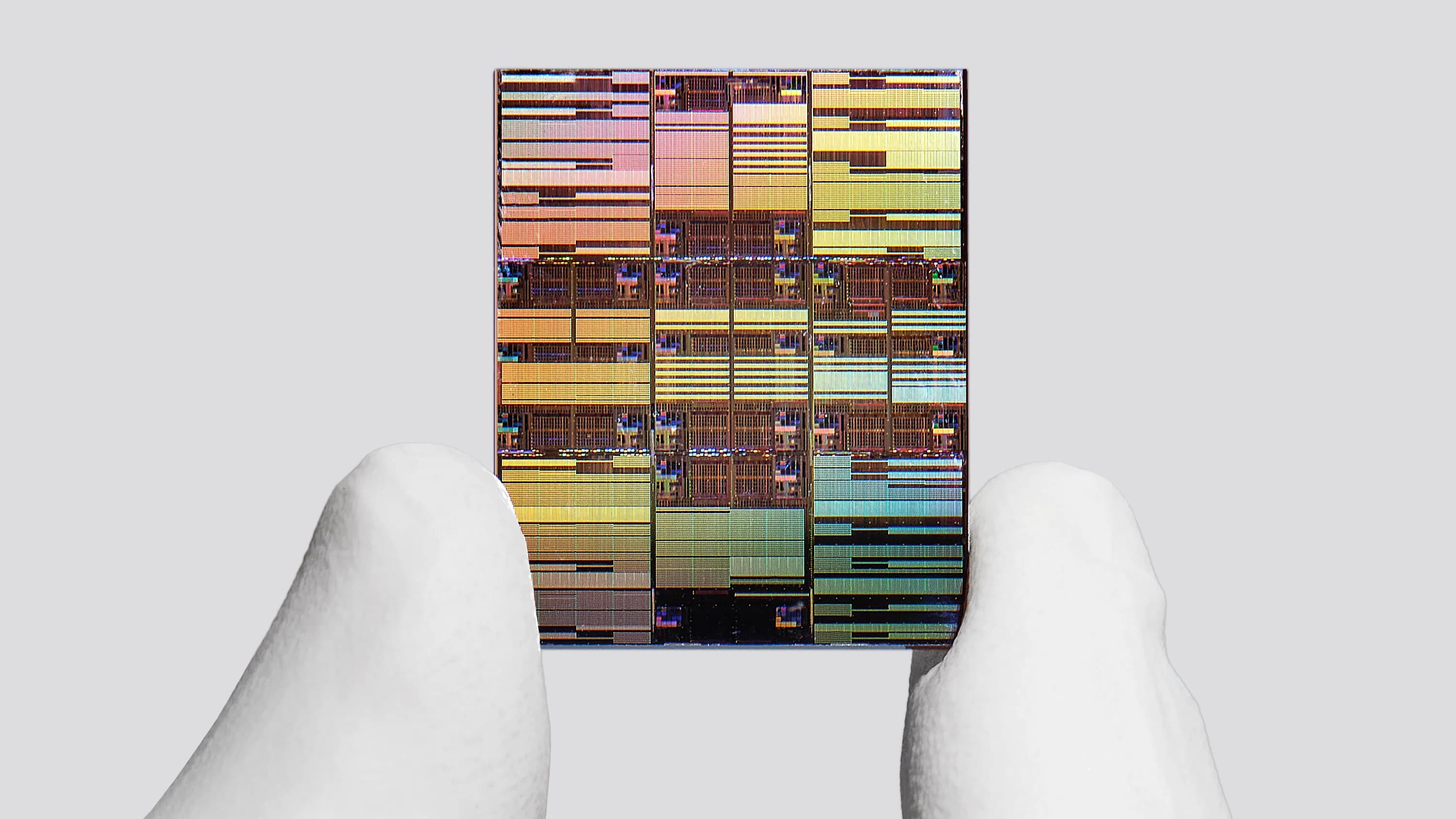
IBM has built a prototype chip with 100 billion transistors on an area the size of a fingernail. The trick: instead of shrinking transistors further, engineers stacked them vertically. The company calls the architecture "nanostack," and it doubles the density of IBM's 2021 state-of-the-art technology while cutting energy use by up to 70%.
"It's not just an incremental step," said Jay Gambetta, director of IBM Research, during a press conference. "It's a meaningful leap forward."
The announcement marks a significant pivot for the semiconductor industry. For decades, chipmakers followed Moore's Law by shrinking transistors to pack more onto each chip. But transistors have now reached sizes where quantum effects start to interfere, just a few dozen nanometers across. They can't get much smaller. So IBM borrowed a page from urban planning: build up.
How the nanostack architecture works
Engineers fabricate the chip layer by layer, like a cake. First, they build transistors on one layer of silicon. Then they place another silicon layer on top and fabricate a second set of transistors directly above the first. Finally, they wire the two layers together.
This vertical stack combines two types of transistors in what's known as a complementary field-effect transistor, or CFET. IBM's approach differs from competitors in one important way: the transistors in the second layer don't sit directly on top of those in the first layer. They're staggered, which IBM says simplifies wiring.
Each transistor's channel consists of three nanosheets, each 15 atoms thick, spaced nine nanometers apart. The architecture builds on nanosheet technology that has been used in state-of-the-art chips since around 2022.
IBM calls this "sub-nanometer" or "0.7 nanometer" technology. But that's a marketing term. It doesn't correspond to any actual physical measurement on the chip. The distance between transistors has stayed at about 40 nanometers for years, according to Qing Cao, a professor of materials science and engineering at the University of Illinois at Urbana-Champaign.
What the performance gains mean
Compared with IBM's previous architecture, chips built with nanostack can do up to 50% more work in the same amount of time. They're also up to 70% more energy efficient. For data centers already struggling with power consumption, those numbers matter.
"Absolutely, it's transformational," said Dan Hutcheson, vice chair of TechInsights, a technology analysis firm. "This puts another 10, 15 years on the roadmap."
Gambetta expects chips with nanostacking to be widely used in data centers within a decade. The improved efficiency could help facilities manage their growing energy demands, particularly as AI workloads continue to scale.
IBM won't make the chips itself
IBM designs chip architecture but doesn't manufacture at scale. The company will partner with semiconductor manufacturers to produce actual chips. It anticipates the design will be used across many chip types, including GPUs and CPUs.
"I expect to have many conversations with designers about how they can use this technology," said Huiming Bu, IBM's vice president of global semiconductor R&D.
IBM isn't alone in pursuing vertical stacking. Intel, Samsung, TSMC, and the Belgian research lab Imec have all been investigating CFETs. But IBM's staggered approach distinguishes its design from the competition.
How this differs from AMD and Huawei's approaches
Other companies have taken different paths to multi-tiered chips. AMD's 3D V-Cache and Huawei's forthcoming LogicFolding technology fabricate transistors on each layer independently, then bond the layers together. IBM's method builds one layer directly on top of the other, allowing more precise alignment. That precision matters because transistors are so small that even minor misalignment degrades performance.
Looking ahead, chipmakers could try stacking more than two tiers. But they'll face significant engineering challenges. Heat dissipation becomes harder as you add layers. Wiring complexity increases. And yields, already difficult at these scales, tend to drop.
The Moore's Law question
Gordon Moore observed in 1965 that the number of transistors on a chip doubles approximately every two years. That observation drove the semiconductor industry for decades. But as transistors approached atomic scales, many predicted Moore's Law would hit a wall.
Vertical stacking offers a detour around that wall. Instead of shrinking transistors, you add more layers. If IBM's claims hold up in production, it could buy the industry another decade or more of density improvements.
The catch: IBM has shown a prototype. Production is another matter. Translating lab results to high-volume manufacturing takes years. And yields at these densities are notoriously difficult to maintain.
Logicity's Take
For AI teams, the 70% efficiency gain is the number to watch. Training large models already strains data center power budgets. More efficient chips could shift the economics of AI infrastructure, potentially making some workloads viable that weren't before. The 10-year timeline to widespread data center adoption aligns with major cloud refresh cycles. Teams planning infrastructure now should factor this in, though production readiness remains uncertain.
Frequently Asked Questions
What is IBM's nanostack chip architecture?
Nanostack is IBM's approach to stacking transistors vertically in two layers on a silicon chip, doubling density without shrinking individual transistors. The layers are staggered rather than directly aligned to simplify wiring.
When will nanostack chips be available commercially?
IBM expects chips with nanostacking to be widely used in data centers within a decade. The company will partner with manufacturers to produce actual chips but hasn't announced specific production timelines.
What does sub-1nm or 0.7nm mean for chip technology?
The 0.7nm designation is a marketing term, not a physical measurement. The actual distance between transistors remains around 40 nanometers. Node names have become increasingly divorced from physical dimensions in recent years.
How does IBM's approach differ from AMD's 3D V-Cache?
AMD fabricates transistors on each layer separately, then bonds the layers together. IBM builds the second layer directly on top of the first, allowing more precise alignment between transistors.
Will this extend Moore's Law?
Industry analysts like Dan Hutcheson of TechInsights say the technology could add 10-15 years to the roadmap for transistor density improvements, though production challenges remain.
Another major chip announcement targeting data center efficiency
Need Help Implementing This?
Have questions about how semiconductor advances affect your AI infrastructure planning? Reach out to Logicity's team for strategic guidance on hardware roadmaps and data center optimization.
Source: MIT Technology Review
Manaal Khan
Tech & Innovation Writer
Produced with AI assistance and reviewed by the Logicity editorial team. Learn more in our Editorial Policy.