Key Takeaways
- The tutorial covers the full process: finding wild clay, stamping 3D printed circuits, painting traces, and firing tablets
- Porcelain already appears in electronic components like capacitors and resistors, making clay a viable PCB substrate
- The project sidesteps commercial china clay and energy-intensive kilns by using open wood fire techniques
Why Clay? The Conflict Mineral Problem
The hacktivists behind Feminist Hacking start from an uncomfortable fact: the hardware in smart devices contains conflict minerals. This is, as they put it, an "open secret" in consumer electronics. Rather than accept this supply chain as inevitable, they asked a different question: can you build working electronics from materials you dig out of the ground yourself?
The answer, it turns out, is yes. Porcelain already plays a role in electronic components. Capacitors, piezo elements, and resistors all use ceramic materials. The leap to clay PCBs is smaller than it sounds.
But the project imposed extra constraints. No commercial china clay. No expensive kilns that drain resources and energy. The solution came from an unlikely source: a pottery artisan who taught them prehistoric firing techniques using open wood fires.
The Process: From Dirt to Functional Board
After spending two days with the craftsperson, the hacktivists learned to source clay locally, work it properly, and fire it into usable substrates. The blog guide walks readers through each step.
Clay collection and preparation comes first. The tutorial emphasizes removing air and impurities to create uniform, consistent material. This matters for electrical properties. Inconsistent clay means inconsistent behavior under current.
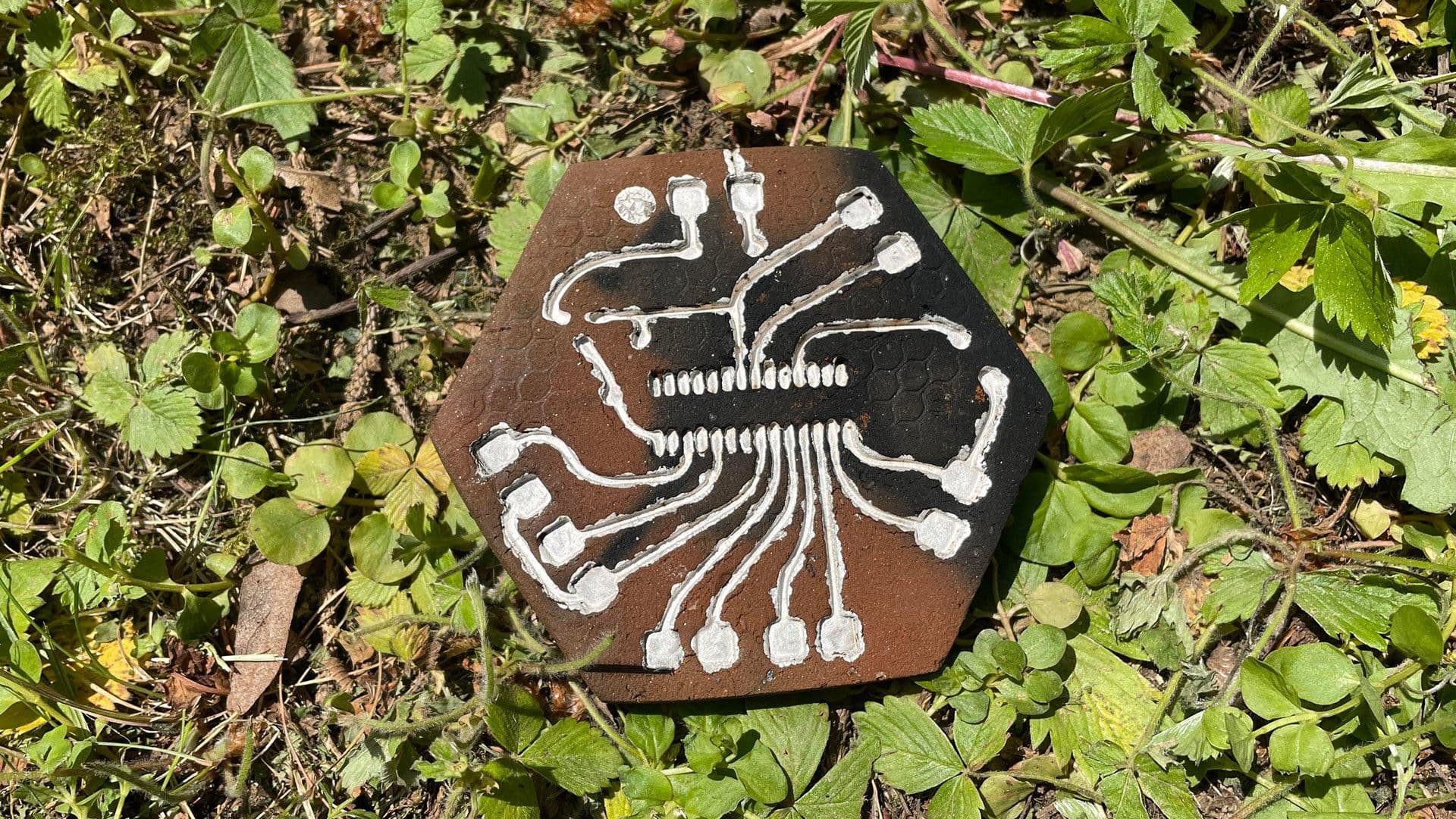
The hacktivists chose a hexagon shape, roughly 10x10cm (about 4x4 inches). This wasn't for aesthetic reasons. Hexagonal cookie cutters are common in ceramic shops. The original plan was to make the boards easy to connect together, but the fired tablet edges proved too imprecise for that idea. It's been shelved for now.
Working with wild clay isn't like working with craft store clay. The material is less elastic and more fragile. Edges may come out rough or split. The guide notes this is fine as long as the inner cutter area stays intact.
Circuit Creation: 3D Printing Meets Ancient Craft
The process blends old and new techniques. 3D printed stamps create circuit patterns on the clay surface. The traces are then painted with conductive material. After firing in an open wood fire, what emerges is a working PCB substrate.
The guide addresses practical concerns throughout. Wild clay behaves differently than commercial ceramics. Firing in wood fires is less predictable than kiln firing. Components may not sit perfectly flat. These aren't bugs to fix but constraints to work within.
Practical Limitations and Real Applications
This isn't a replacement for mass manufacturing. The tolerances can't match commercial PCB fabs. The process takes days rather than hours. Each board is handmade.
But that's not the point. The project demonstrates that electronics don't have to depend entirely on industrial supply chains. For artists, makers, and educators, clay PCBs offer a way to build working circuits while understanding materials at a fundamental level.
The ethical dimension matters too. By sourcing materials locally and using renewable fuel for firing, the project sidesteps questions about where minerals came from and who was harmed extracting them.
Another creative technical project pushing boundaries of unconventional methods
What's Next for Wild Clay Electronics
The Feminist Hacking collective presents this as a starting point, not a finished product. The hexagonal connection idea was dropped because fired edges weren't precise enough. That suggests future iterations could solve the problem with different shapes or finishing techniques.
For electronics enthusiasts willing to get their hands dirty, literally, the full tutorial is available on their blog. It covers clay collection, preparation, stamping, painting, and firing in enough detail to replicate the process.
Logicity's Take
Frequently Asked Questions
Can clay PCBs actually conduct electricity?
Yes. The clay serves as a substrate, while painted conductive traces carry current. The principle is similar to commercial ceramic-based components already used in capacitors and resistors.
What clay works for making PCBs?
The tutorial uses locally sourced wild clay, properly prepared to remove air and impurities. Commercial china clay also works but defeats the ethical sourcing goals of the project.
Do you need a kiln to fire clay PCBs?
No. The hacktivists specifically used prehistoric open wood fire techniques to avoid the energy costs and infrastructure of kiln firing.
How precise are clay PCBs compared to commercial boards?
Less precise. The fired edges can be rough or split, and tolerances won't match commercial PCB fabrication. This limits complexity but doesn't prevent working circuits.
Where can I find the full clay PCB tutorial?
The complete guide is published on the Feminist Hacking blog under the title "MaKING Printed Circuit Boards with Wild Clay."
Need Help Implementing This?
Source: Latest from Tom's Hardware
Huma Shazia
Senior AI & Tech Writer
Produced with AI assistance and reviewed by the Logicity editorial team. Learn more in our Editorial Policy.