Key Takeaways
- IBM's 0.7nm transistor tech packs 100 billion transistors on a fingernail-sized chip, double its 2021 design
- The 'nanostack' architecture stacks transistors vertically instead of flat, a fundamental shift in chip design
- Commercial production is at least five years away, with no manufacturing partner announced yet
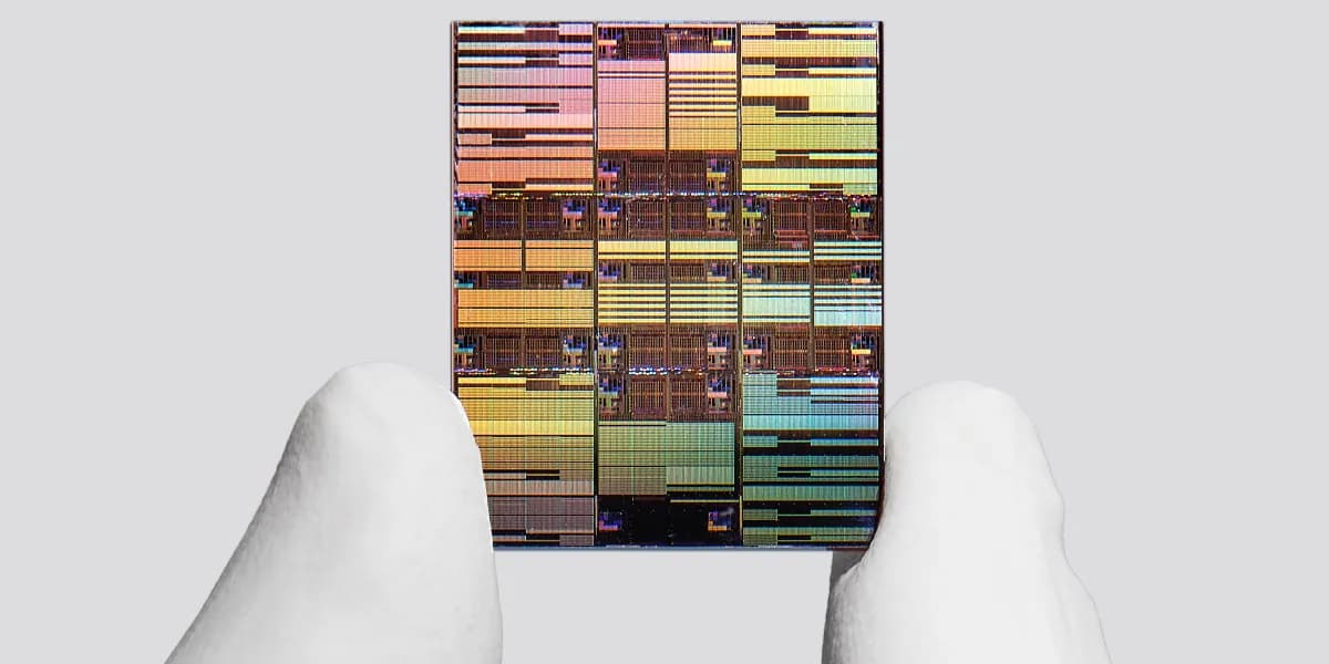
IBM announced what it calls the first chip technology capable of producing transistors smaller than one nanometer, a threshold that seemed physically impossible a decade ago. The 0.7 nanometer design, roughly seven angstroms wide, uses a novel vertical stacking approach that could keep Moore's Law on life support for another generation. IBM's stock jumped 6% in premarket trading on the news.
The key innovation is what IBM calls the 'nanostack' architecture. Traditional chip designs arrange transistors flat, side by side. IBM's approach stacks them vertically in three dimensions, cramming more switching capacity into the same physical footprint. The result: nearly 100 billion transistors on a surface the size of a fingernail.
How does nanostack compare to current chips?
IBM's 2021 breakthrough was the 2-nanometer chip. This new design roughly doubles that density while delivering up to 50% higher performance or 70% greater energy efficiency, depending on how manufacturers optimize the process. For context, TSMC and Samsung currently mass-produce chips at 3nm, while Intel just moved its 1.8nm process into risk production last week.
The performance claims matter most for AI workloads, where energy efficiency translates directly to cost. Training large language models requires enormous computational resources. Data centers running AI workloads face power constraints as much as silicon constraints. A chip that does the same work with 70% less energy changes the economics of model training.
“With our new nanostack architecture, we're not just making smaller transistors, we're reinventing how chips are built to deliver dramatically more power and energy efficiency.”
— Jay Gambetta, Director of IBM Research
When will these chips actually ship?
Not soon. IBM says production could begin within five years, which in semiconductor terms means somewhere between 2029 and 2030 at the earliest. That timeline assumes everything goes right, and in chip manufacturing, things rarely do.
IBM also hasn't named a manufacturing partner. The company previously licensed its chip technologies to Samsung and Japan's Rapidus, but neither has been announced for the sub-1nm process. This matters because IBM doesn't manufacture chips at scale. It designs them and licenses the technology to foundries that can actually build millions of units.
The gap between laboratory demonstration and mass production is where many promising chip technologies die. IBM has a strong track record of chip research breakthroughs, but translating those breakthroughs into commercial products requires billions in capital equipment and years of process refinement.
The race to extend Moore's Law
Intel, TSMC, and Samsung have all announced roadmaps pushing toward 1nm and beyond. The challenge isn't just shrinking transistors. At atomic scales, quantum effects cause electrons to tunnel through barriers they shouldn't be able to cross. Heat dissipation becomes harder. Manufacturing defects that would be invisible at larger scales ruin entire chips.
Vertical stacking, IBM's approach, is one path forward. TSMC has also explored 3D transistor designs, though with different architectures. Intel's ribbon transistors take yet another approach. Nobody knows which design will dominate, and the answer might be different for different applications.
What's clear is that AI workloads are driving this competition. Before 2020, chip improvements were nice to have. After ChatGPT, they're existential. Nvidia's data center revenue tripled in a year because customers couldn't get enough compute. Whoever cracks the next generation of chip manufacturing will capture an enormous share of a market projected to exceed $200 billion.
What this means for IBM's business
IBM's stock has fallen about 11% this year despite strong AI rhetoric across the industry. The company's cloud and software businesses have struggled to match the growth rates of Microsoft, Amazon, and Google. A chip technology breakthrough doesn't immediately change that picture. IBM licenses technology; it doesn't capture the full value of manufacturing.
But it does give IBM leverage. Samsung and Rapidus need cutting-edge designs to compete with TSMC. If IBM's nanostack architecture proves manufacturable, licensing fees could become a meaningful revenue stream. More importantly, it keeps IBM relevant in the AI infrastructure conversation.
Logicity's Take
IBM's announcement is real research, not vaporware, but the five-year production timeline is the key detail. For companies planning AI infrastructure today, this changes nothing about procurement decisions. Current 3nm and 5nm chips from TSMC and Samsung remain the practical choice. Watch for IBM's manufacturing partnership announcement. If they sign with TSMC, that signals confidence in scalability. If they stick with smaller partners like Rapidus, expect a longer path to volume production. The technology is impressive, but chip breakthroughs only matter when they ship.
Earlier coverage of IBM's vertical transistor research
Frequently Asked Questions
What is IBM's nanostack chip technology?
Nanostack is a transistor architecture that stacks transistors vertically in three dimensions rather than arranging them flat. This allows IBM to fit nearly 100 billion transistors on a fingernail-sized chip at 0.7nm scale.
How small is 0.7 nanometers?
0.7 nanometers equals 7 angstroms. For reference, a single silicon atom is about 0.2 nanometers wide, so IBM's transistors are roughly three to four atoms across at their smallest dimension.
When will sub-1nm chips be available commercially?
IBM estimates production could begin within five years, meaning 2029 or 2030 at earliest. The company has not yet announced a manufacturing partner for the technology.
How does this compare to Intel and TSMC chips?
TSMC and Samsung currently manufacture at 3nm, while Intel's 1.8nm process just entered risk production. IBM's 0.7nm technology is still in the research phase, not production.
Why does this matter for AI?
AI model training requires enormous computational power and energy. IBM claims the new chips offer up to 50% higher performance or 70% better energy efficiency, which directly reduces the cost of running AI workloads.
Need Help Implementing This?
Planning AI infrastructure for your organization? Contact Logicity's advisory team for vendor-neutral guidance on chip roadmaps, cloud compute options, and hardware procurement strategies.
Source: Tech-Economic Times / ET
Manaal Khan
Tech & Innovation Writer
Produced with AI assistance and reviewed by the Logicity editorial team. Learn more in our Editorial Policy.