Architect Labs raises $24M to speed custom chip design with AI
Key Takeaways
- Architect Labs raised $24 million in seed funding to automate custom chip design using AI
- The startup aims to compress the typical two-year, hundreds-of-millions-dollar chip development cycle
- Investors include Kindred Ventures, Google DeepMind's Jeff Dean, and executives from OpenAI and Nvidia
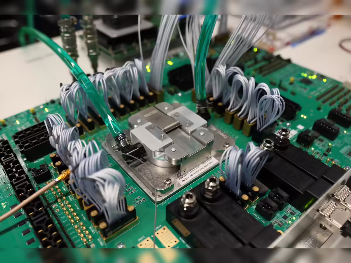
Architect Labs, a Palo Alto startup, announced Thursday it raised $24 million in seed funding to build an AI-powered platform for custom chip design. The company is taking aim at Broadcom and Marvell, two firms that dominate the lucrative business of designing custom silicon for cloud giants like Amazon and Google.
The pitch is straightforward: custom chips currently take about two years to design and cost hundreds of millions of dollars in engineering labor and R&D. Architect Labs claims its AI can compress that timeline significantly, making bespoke silicon accessible to companies that would otherwise rely on off-the-shelf hardware from Nvidia.
Who is backing this bet?
Kindred Ventures led the round, with participation from TQ Ventures, Race Capital, and Together Fund. The investor list includes some heavy hitters from the AI world: Jeff Dean, chief scientist at Google DeepMind, along with unnamed executives from OpenAI and Nvidia.
That roster matters. Building an AI system that can reliably design silicon is a hard problem sitting at the intersection of machine learning and hardware engineering. Having Dean's backing signals that serious people believe Architect's approach is technically viable.
What problem is Architect Labs solving?
Co-founder Ebrahim Hussain told Reuters that the hardest part of custom chip development is not the backend layout or manufacturing. The real bottleneck is architecture exploration: figuring out how to translate a specific workload, whether AI inference, robotics, or something else, into efficient silicon.
"Their biggest problem today is not necessarily the backend execution or the layout," Hussain said. "Their biggest thing is how can I take this workload that I want to deliver to the world, whether it be AI or robotics or anything like that, and how can I build the chip architecture."
Traditional electronic design automation tools from Synopsys and Cadence help with parts of this process, but they require armies of specialized engineers working for months or years. Architect wants AI agents to handle the exploration and verification steps, producing designs that are, in their words, "correct by construction."
How big is the market they're targeting?
Broadcom and Marvell's custom chip businesses generate tens of billions of dollars annually. Their clients are the hyperscalers: Amazon Web Services, Google Cloud, Microsoft Azure. These companies want silicon optimized for their specific workloads because even small efficiency gains translate to massive savings at datacenter scale.
But Architect is not just targeting the hyperscalers. Hussain said the company also plans to work with software companies that could benefit from custom hardware to run their applications faster or more efficiently. This is a wider aperture than the existing Broadcom/Marvell model, which focuses on the biggest clients who can afford the time and cost.
The team and the TSMC comparison
Architect Labs was founded by Hussain and Aaditya Subedi. The company currently has about 18 employees, split between machine learning specialists and hardware engineers. Early community discussions on Reddit have highlighted the team's pedigree, with engineers reportedly drawn from Anthropic, Meta, Tesla, and DeepMind.
Subedi offered an ambitious comparison: the goal is to make chip design as accessible as TSMC has made chip manufacturing. That is a bold claim. TSMC spent decades and hundreds of billions of dollars becoming the world's foundry, and its manufacturing expertise remains essentially unmatched. Whether AI can do something similar for the design side is an open question.
What are the skeptics saying?
On Hacker News, discussions have focused on whether "correct-by-construction" chip design is actually achievable with current AI capabilities. Verification is one of the hardest problems in hardware engineering. A single bug in silicon can mean millions of dollars in wasted fabrication costs and months of delays.
There is also the question of whether Architect can truly outperform the established EDA tools that have been refined over decades. Synopsys and Cadence are not standing still; they are integrating machine learning into their own products. Architect's bet is that a fresh approach, built from the ground up around AI, will move faster than incremental improvements to legacy systems.
Why this matters now
The demand for custom silicon has never been higher. AI workloads are pushing the limits of general-purpose chips, and companies are increasingly willing to invest in hardware tailored to their specific needs. Nvidia dominates the GPU market, but its products are designed for broad compatibility, not maximum efficiency on any single task.
If Architect can deliver on its promise, even partially, it could open up custom chip design to a much larger pool of customers. Companies that currently cannot afford the time or money to work with Broadcom or Marvell might suddenly have an option.
Logicity's Take
The $24 million seed is small relative to the market Architect is targeting, but it is enough to prove the concept. The real test is whether their AI can produce designs that actually tape out successfully. If Architect can demonstrate even one production chip designed primarily by AI, the valuation will jump dramatically. The risk is that chip design is one of those domains where 90% accuracy is worthless; it needs to be right, or the silicon is scrap.
Frequently Asked Questions
What does Architect Labs do?
Architect Labs uses artificial intelligence to automate and accelerate custom chip design, targeting a process that currently takes about two years and costs hundreds of millions of dollars.
Who invested in Architect Labs?
Kindred Ventures led the $24 million seed round, with participation from TQ Ventures, Race Capital, Together Fund, Google DeepMind's Jeff Dean, and executives from OpenAI and Nvidia.
How does Architect Labs compete with Broadcom and Marvell?
While Broadcom and Marvell use large teams of engineers over multi-year timelines, Architect Labs aims to use AI agents to dramatically reduce both the time and cost of custom chip development.
Where is Architect Labs based?
The company is headquartered in Palo Alto, California, and has approximately 18 employees working across machine learning and hardware engineering.
Another AI company expanding into unexpected hardware territory
Need Help Implementing This?
Logicity covers the technologies reshaping enterprise infrastructure. For custom chip design updates, AI hardware developments, and deep dives into the compute stack, subscribe to our newsletter or reach out to our editorial team.
Source: Tech-Economic Times / ET
Huma Shazia
Senior AI & Tech Writer
Related Articles
Browse all
Robotaxi Companies Are Hiding How Often Humans Take the Wheel
Autonomous vehicle firms like Waymo and Tesla are under scrutiny for refusing to disclose how often remote operators step in to control their self-driving cars. A Senate investigation reveals major gaps in transparency, raising safety and accountability concerns.

Wisconsin Governor Throws a Wrench in Age Verification Plans
Wisconsin Governor Tony Evers has vetoed a bill that would have required residents to verify their age before accessing adult content online, citing concerns over privacy and data security. This move comes as several other states have already implemented similar age check requirements. The veto has significant implications for the future of online age verification.

Apple's App Store Empire Under Siege: The Battle for the Future of Tech
The long-running feud between Apple and Epic Games has reached a boiling point, with Apple preparing to take its case to the Supreme Court. The tech giant is fighting to maintain control over its App Store, while Epic Games is pushing for more freedom for developers. The outcome could have far-reaching implications for the entire tech industry.

Tesla's Remote Parking Feature: The Investigation That Didn't Quite Park Itself
The US auto safety regulators have closed their investigation into Tesla's remote parking feature, but what does this mean for the future of autonomous driving? We dive into the details of the investigation and what it reveals about the technology. The National Highway Traffic Safety Administration found that crashes were rare and minor, but the investigation's closure doesn't necessarily mean the feature is completely safe.