Samsung Shows HBM5 Mockup With Heat Path Block Cooling
Key Takeaways
- Samsung's HBM5 will use a 2nm base die, down from 4nm in HBM4
- Heat Path Block cooling pulls heat from inside the memory stack via thermal pillars
- Both Samsung and SK hynix are targeting the same thermal bottleneck at the die-to-die interface
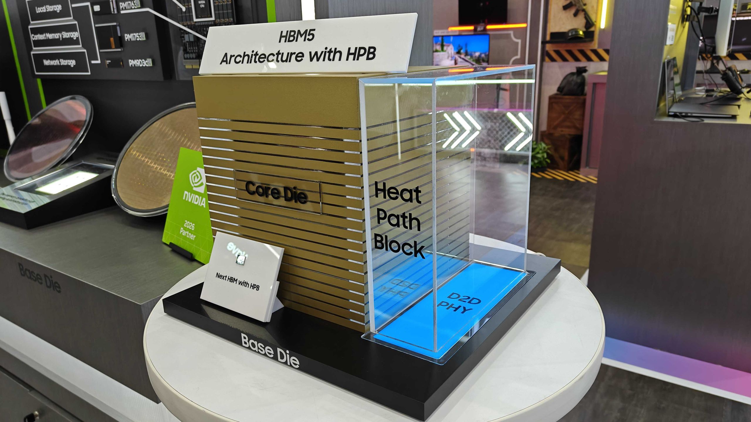
Samsung brought its first physical HBM5 memory mockup to Computex 2026 in Taipei this week. The company paired its eighth-generation AI memory with a new cooling structure called Heat Path Block, or HPB. The timing matters: SK hynix unveiled its own thermal design, iHBM, just last week. Both Korean memory giants are now racing to solve the same heat problem.
The thermal bottleneck both companies are chasing
The problem sits at the die-to-die (D2D) PHY layer. This high-speed link connects the HBM base die to the GPU. As memory stacks grow taller and run faster, power density and temperatures at this interface climb exponentially. Traditional cooling methods that let heat escape outward through the core dies are hitting their limits.
Samsung's Heat Path Block takes a different approach. Instead of passive heat dissipation, HPB builds thermal pillars inside the memory stack. These pillars pull heat from the D2D interface and carry it to a spreader positioned above or beside the package. Think of it as a set of chimneys running through the stack rather than relying on heat to find its own way out.
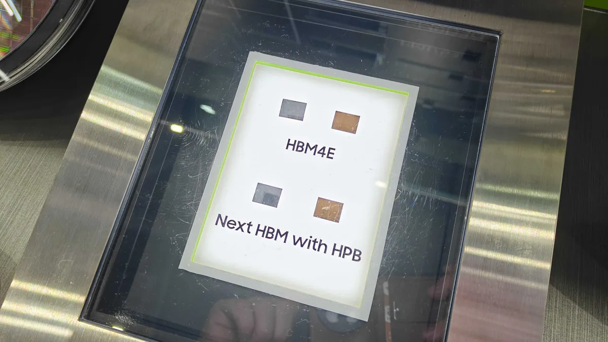
2nm base die and HBM4E progress
Samsung confirmed a significant manufacturing upgrade: HBM5's base logic die will be fabricated on the company's in-house 2nm process. That's a full node shrink from the 4nm used in HBM4 and HBM4E. The smaller process should improve power efficiency, but it also gives Samsung vertical integration advantages. The company runs both a memory business and a logic foundry, letting it build the entire HBM5 stack internally.
The company has already validated HPB on the current generation. Samsung said it implemented and verified the cooling technology on HBM4E, whose first 12-layer samples began shipping last month. Those HBM4E chips run at 14 Gbps, scaling to 16 Gbps, with 3.6 TB/s bandwidth per stack.
“AI systems are becoming more powerful and densely integrated, making heat management, data-processing efficiency, and packaging stability just as important as memory performance itself.”
— Song Jai-hyuk, President and CTO of Samsung's Device Solutions division
How SK hynix is solving the same problem differently
SK hynix arrived at the same bottleneck via a different route. Its iHBM design embeds cooling elements directly at the D2D PHY layer hotspot. The elements use electrically non-conductive but thermally conductive silicon. SK hynix claims this approach cuts thermal resistance by more than 30% compared to current products.
The engineering philosophies differ. Samsung's HPB creates dedicated heat channels running through the stack. SK hynix's iHBM places cooling material right where the heat generates. Both target the same interface, but the manufacturing and yield implications could diverge significantly.
Why both companies are solving this now
A roadmap from KAIST (Korea Advanced Institute of Science and Technology) projected HBM5 specifications that explain the urgency. The next generation is expected to reach a 4,096-bit interface, roughly 4 TB/s bandwidth per stack. Per-stack power consumption could hit around 100 watts. That thermal load makes current packaging approaches unworkable.
Both Samsung and SK hynix are reworking their thermal designs now rather than scrambling at launch. AI accelerator manufacturers like Nvidia need reliable thermal performance guarantees before committing to memory suppliers. Song said Samsung would continue building its competitiveness through cooperation with partners, including Nvidia.
Related thermal engineering innovation in the cooling space
What the technical community is debating
Discussion on Reddit's r/hardware and Hacker News has focused on manufacturing complexity. The thermal pillar structures in HPB and the embedded cooling elements in iHBM both add steps to an already difficult stacking process. Some engineers worry about yield impacts. Others argue these in-package solutions represent the inevitable workaround as AI memory pushes against physical limits.
The debate highlights a broader shift in semiconductor manufacturing. Memory performance used to mean faster speeds and higher density. Now thermal management has become a primary engineering constraint, not a secondary consideration.
Timeline and competitive implications
Mass production of Samsung's HBM5 is anticipated around 2028. SK hynix has not announced a specific timeline but is working on similar schedules. The two companies supply the vast majority of HBM to AI chip makers. Micron remains a distant third in the market.
For Nvidia, AMD, and other accelerator companies, the thermal race between Samsung and SK hynix matters directly. Whichever supplier delivers reliable high-bandwidth memory with better thermal characteristics will likely capture larger portions of the AI training chip market.
AI hardware development requiring high-bandwidth memory
Logicity's Take
Frequently Asked Questions
What is Samsung's Heat Path Block (HPB) cooling?
HPB builds thermal pillars inside the HBM memory stack that pull heat from the die-to-die interface and carry it to a heat spreader above or beside the package. It targets the D2D PHY layer where temperatures spike as stacks grow taller.
How does Samsung's HBM5 cooling compare to SK hynix's iHBM?
Samsung's HPB creates dedicated heat channels through the stack. SK hynix's iHBM embeds thermally conductive silicon directly at the hotspot. Both target the same thermal bottleneck but use different engineering approaches.
What process node will Samsung use for HBM5?
Samsung confirmed HBM5's base logic die will be manufactured on its 2nm process, a full node shrink from the 4nm used in HBM4 and HBM4E.
When will Samsung HBM5 be available?
Mass production is anticipated around 2028. Samsung has already validated the HPB cooling technology on HBM4E, which began shipping in 12-layer samples last month.
Why is thermal management critical for next-gen AI memory?
HBM5 is projected to consume around 100 watts per stack while delivering 4 TB/s bandwidth. Current passive cooling cannot handle this thermal load, making active in-package cooling solutions necessary.
Need Help Implementing This?
Source: Latest from Tom's Hardware
Huma Shazia
Senior AI & Tech Writer
اقرأ أيضاً

رأي مغاير: كيف يؤثر اختراق الأمن الداخلي الأميركي على شركاتنا الخاصة؟
في ظل اختراق عقود الأمن الداخلي الأميركي مع شركات خاصة، نناقش تأثير هذا الاختراق على مستقبل الأمن السيبراني. نستعرض الإحصاءات الموثوقة ونناقش كيف يمكن للشركات الخاصة أن تتعامل مع هذا التهديد. استمتع بقراءة هذا التحليل العميق

الإنسان في زمن ما بعد الوجود البشري: نحو نظام للتعايش بين الإنسان والروبوت - Centre for Arab Unity Studies
في هذا المقال، سنناقش كيف يمكن للبشر والروبوتات التعايش في نظام متكامل. سنستعرض التحديات والحلول المحتملة التي تضعها شركات مثل جوجل وأمازون. كما سنلقي نظرة على التوقعات المستقبلية وفقًا لتقرير ماكنزي

إطلاق ناسا لمهمة مأهولة إلى القمر: خطوة تاريخية نحو استكشاف الفضاء
تعتبر المهمة الجديدة خطوة هامة نحو استكشاف الفضاء وتطوير التكنولوجيا. سوف تشمل المهمة إرسال رواد فضاء إلى سطح القمر لconducting تجارب علمية. ستسهم هذه المهمة في تطوير فهمنا للفضاء وتحسين التكنولوجيا المستخدمة في استكشاف الفضاء.